Electrostatic CRT Tester — Mark 2 · Volume 4
Electrostatic CRT Tester — Vol 4: Inside the Tester — Circuit Theory
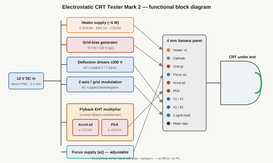
One 12 V rail in, a gun's worth of voltages out — tracing every supply from the barrel jack to the banana panel
4.1 A note on what is and isn’t public
Before we dissect anything: the maker (sgitheach.org.uk) releases this as a fully open design under CC BY-SA 4.0, but the detailed schematic, the BOM, and the Gerbers live in the project’s Dropbox folders, not on the web pages. This volume was written without that schematic in hand. So where a specific part value or topology is not published, I do not invent an IC part number or pretend to quote a net that I have not seen. Instead I reason from the published specification — the numbers in Vol 2’s electrode table, the stated 12 V input, the ~6 W heater ceiling, the ±300 V and kV rails — and from standard high-voltage / analog design practice, and I flag every such inference as a design-reasoned conclusion rather than a read-from-schematic fact. When Jeff opens the Dropbox schematic on the bench, the block-level architecture here will be correct; individual component designators are his to fill in against the real board.
That honesty is not a hedge — it is the useful engineering posture. The interesting question is not “what is U7?” but “given the spec, what must this stage be doing, and what are the design constraints that force it?” That question we can answer rigorously.
4.2 The whole design premise: one low-voltage rail in
Everything in this instrument follows from a single decision the maker made explicit: “Simple and manually operated — no micro-controller or PC in sight,” fed from one 12 V DC bench supply through a 2.1 mm barrel jack. Understand that decision and the rest of the circuit falls out of it.
Consider what an electrostatic CRT actually demands, all at once (this is the Vol 2 electrode table, condensed):
Table 1 — Consider what an electrostatic CRT actually demands, all at once (this is the Vol 2 electrode table, condensed)
| Electrode | Potential it needs | Current it draws |
|---|---|---|
| Heater | 2.5–6.3 V AC/DC | 0.6–2 A (this is where the watts go) |
| Grid g1 | −5 to −120 V | ~microamps (it is a bias, draws ~no current) |
| Focus a1 | hundreds of V to ~1 kV | ~zero (voltage-set electrode) |
| Accel a2 | up to +2.2 kV | ~sub-milliamp beam current |
| PDA | up to +5.6 kV | ~sub-milliamp |
| X/Y plates | −300 to +300 V differential | ~zero DC (capacitive plates) |
The naïve way to make all of that is the way the maker used to do it, and says so on the site: a bench littered with separate supplies — “a couple of old Heathkit IP17 high-voltage supplies, a separate EHT supply.” That works, but it is four or five mains-powered boxes, four or five sets of leads, four or five ground references to get wrong, and no single point at which the whole gun comes up and down together. The Mark 2 collapses all of it onto one PCB that takes 12 V in and synthesises every other potential on-board.
Why is that the whole point, and not just tidiness?
- One ground, one reference. Every derived rail on the board shares the cathode-return reference. The grid’s −60 V, the accel’s +2.2 kV, and the plates’ ±300 V are all defined against the same node, which is exactly the relationship the tube cares about. Stitch five separate supplies together on the bench and you are hand-building that common reference out of banana leads and hoping.
- One safe input. The only thing that crosses from the mains world into this box is a 12 V DC brick. The lethal voltages — the kV EHT, the ±300 V — are all generated inside the instrument from that harmless input and never leave it except on the clearly-labelled EHT banana jacks. There is no mains transformer, no line-voltage primary, nothing at 120/240 V AC anywhere on the board.
- One power budget. Because it all comes from 12 V, the total draw is bounded and knowable (next section). You can run the whole thing off a modest lab supply, or a sealed-lead-acid battery, or a 12 V 3–4 A wall brick.
- Portability and repeatability. A single box you can carry to the tube, set up identically every time, and bring the whole gun up with a known sequence (Vol 6).
The cost of that elegance is that the board has to do real power-electronics work internally — a DC-DC boost/flyback stage to manufacture kilovolts from 12 V — and that stage is the most interesting circuit in the instrument.
4.3 Power budget from the 12 V input
Everything the board can do is bounded by what 12 V DC through a barrel jack can deliver. Let us size it.
The heater dominates. The spec caps heater output at ~6 W — explicitly “6.3 V @ 0.6 A, 4 V @ 1.1 A, or 2.5 V @ 2 A,” each of which is ~3.8–5.0 W at the tube (6.3 V × 0.6 A = 3.8 W; 4 V × 1.1 A = 4.4 W; 2.5 V × 2 A = 5.0 W) under a ~6 W design ceiling. This is by far the largest single load in the box. Everything else — grid bias, focus, the beam current through the EHT rails, the deflection plates — draws either microamps or sub-milliamps at its respective voltage, so their power is small even though their voltage is large.
Run the arithmetic for the worst-case heater setting, 2.5 V @ 2 A:
  Heater output power     P_htr  = 2.5 V × 2.0 A            = 5.0 W
  If the heater rail is a linear/dropper stage from 12 V:
    input current          I_in  = 2.0 A (series-pass) — but
    dropper dissipation    P_drop = (12 − 2.5) V × 2.0 A    = 19.0 W  ← ugly
That 19 W of dissipation in a linear pass element is the tell that the heater rail is almost certainly not a brute linear dropper for the high-current/low-voltage settings — you would need a serious heatsink and you would be throwing away three-quarters of your input power as heat. Design-reasoning from the spec: the heater supply is much more likely a switching (buck) converter, or a switched/PWM current-limited stage, that steps 12 V down to the selected heater voltage efficiently and enforces the ~6 W / current ceiling. A buck at ~85–90 % efficiency delivering 5 W draws only:
  Buck input power        P_in  ≈ 5.0 W / 0.88               ≈ 5.7 W
  Buck input current      I_in  ≈ 5.7 W / 12 V               ≈ 0.47 A
That is a far friendlier number and consistent with a board that expects a modest 12 V brick.
Now the rest of the box. Sum the small loads:
Table 2 — Now the rest of the box. Sum the small loads
| Load from 12 V | Output | Approx. output power | Notes |
|---|---|---|---|
| Heater (worst case) | 2.5 V @ 2 A | ~5 W | The one real load |
| EHT stack (a2 + PDA) | +2.2 kV & +5.6 kV @ sub-mA beam | ~1–3 W into the flyback | Beam current is small; most input power covers switching + multiplier losses |
| Grid-bias rail | −5…−120 V @ µA | ≪ 0.1 W | Bias node, negligible |
| Focus divider (a1) | high-V @ ~0 A | ≪ 0.1 W | Voltage-set, draws leakage only |
| ±300 V deflection rails | ±300 V, capacitive load | small; mostly quiescent | Plates take no DC current |
| Control / bias / feedback | — | ~0.5–1 W | Op-amps, references, feedback dividers |
Total design-reasoned draw: the instrument as a whole is plausibly a ~8–12 W load on the 12 V rail — call it ~1 A typical, budget for 2–3 A to cover heater inrush, the flyback’s peak primary current, and converter startup. That is why the spec calls for a 12 V DC bench PSU and nothing exotic: any 12 V / 3 A supply carries it comfortably. A reader wiring this up should give it a supply that can source at least ~2–3 A without folding back, because the flyback primary and the heater converter both present pulsed/inrush current that a marginal wall-wart will sag under.
Design note — why 12 V and not, say, 24 V? 12 V is the universally-available bench/automotive rail, and it is low enough to be intrinsically safe to handle while being high enough that a flyback with a reasonable turns ratio can reach multi-kV secondary swings without an absurd number of multiplier stages. Push the input lower (5 V USB) and the flyback turns ratio and primary current both get uncomfortable for kV output; go higher (48 V) and you lose the “any bench, any battery” convenience. 12 V is the sweet spot for a hand-built EHT generator.
4.4 The flyback EHT multiplier — the heart of the box
This is the circuit that justifies the whole architecture: it manufactures +2.2 kV (accel, a2) and +5.6 kV (PDA) from a 12 V input. The maker names the flyback transformer as the key custom component — it is the one part you cannot buy off a distributor shelf, which is exactly why the “minimum kit” (£50) is “PCB + flyback transformer only”: they give you the hard-to-source magnetics and the board, and you find everything else. That pricing tells you where the design’s irreplaceable IP sits.
4.4.1 How a flyback stage makes high voltage
A flyback converter is a transformer-isolated DC-DC topology that stores energy in the transformer’s magnetising inductance during the switch on-time and dumps it into the secondary during the off-time. It is the natural choice for high-voltage generation because (a) the transformer turns ratio gives you a first big step-up for free, and (b) the “flyback” voltage spike when the primary current is interrupted is itself a step-up mechanism you then rectify.
The cycle, from 12 V:
- On-time (switch closed). The primary is connected across the ~12 V rail. Current ramps up linearly in the primary,
di/dt = V/L_p, storing energyE = ½·L_p·I_peak²in the core’s magnetic field. During this phase the secondary diode is reverse-biased — no energy reaches the output; the core is charging. - Off-time (switch opens). Primary current is abruptly interrupted. The collapsing flux induces a voltage in both windings whose polarity now forward-biases the secondary rectifier. The stored energy transfers to the secondary/output. The secondary voltage during flyback is the primary flyback voltage times the turns ratio
N_s/N_p— and with a high step-up ratio that is already hundreds of volts to a kilovolt or more per pulse. - Rectify and multiply. That pulsed secondary output is rectified and, crucially, fed into a diode–capacitor voltage multiplier ladder (a Cockcroft–Walton / Villard cascade) that stacks the rectified peaks to reach the final +2.2 kV and +5.6 kV. Each stage of the ladder adds roughly one peak-to-peak of the drive to the DC output, so a modest secondary swing multiplied over several stages gets you to multi-kV without demanding an insane transformer turns ratio or insanely high volts on any single winding.
The reason this topology is right for a CRT tester specifically: the loads are tiny (sub-milliamp beam current), so the flyback need only deliver a fraction of a watt to the EHT nodes. A multiplier ladder is efficient and cheap at low current but has terrible regulation at high current (its output impedance is dominated by the stage capacitances and switching frequency). For a beam that draws micro-to-milliamps, that high output impedance is fine — and it is even a mild safety feature, since a multiplier stiff enough to hold kV into a short would be far more dangerous.
4.4.2 ASCII schematic — flyback + multiplier ladder
Here is the block-and-ladder architecture, design-reasoned from the spec (part designators are illustrative, not read from the maker’s schematic):
   +12V ──┬─────────────┐
          │             │  Np          Ns (high-ratio step-up)
          │           ╭──┴──╮ ┊┊ ╭──────┴───────┐
     [feedback]       │     │ ┊┊ │              │
      sense           │  o  ║ ┊┊ ║  o           │
        │             │  o  ║ ┊┊ ║  o           ●── secondary "hot" node
        │             ╰──┬──╯ ┊┊ ╰──────┬───────┘   (pulsed, hundreds of V/pk)
        │                │  flyback xfmr │
        │              ┌─┴─┐             │
        │   PWM/osc → ─┤SW │ (MOSFET)    │      COCKCROFT–WALTON LADDER
        │              └─┬─┘             │   (each stage ≈ +1× pk to the DC out)
        │                │               │
        │               GND      ┌───┬───┬───┬───┬───┬── ... ──► +5.6 kV  (PDA tap)
        │                        │Ca │Cb │Cc │Cd │Ce │
        └───── ctrl loop ────    ─┴─D─┴─D─┴─D─┴─D─┴─D─┴──────┐
                (regulates via     ▽   ▽   ▽   ▽   ▽         │
                 an ADJUST pot)   diodes stacking the peaks  │
                                          │                  │
                            (intermediate node) ──► +2.2 kV  (a2 tap)
                                          │
                                         GND (cathode reference)
Read it left to right: 12 V into the primary; a MOSFET switch chopped by an oscillator/PWM stage; the flyback transformer stepping up and inverting energy into the secondary on each off-cycle; a diode–capacitor ladder rectifying and stacking the pulses up to +5.6 kV at the top of the stack, with the +2.2 kV accel tap brought out from an intermediate node partway up the ladder. A feedback path senses the output (through a very-high-value resistive divider — you cannot hang an ordinary divider on 5.6 kV without gigohms) and closes the loop back to the PWM to regulate the EHT, with an ADJUST pot setting the target so the operator can dial a2 (and hence beam energy / deflection sensitivity) to suit the tube.
4.4.3 Why the flyback is “the custom component”
Three reasons the transformer is the irreplaceable part and everything else is commodity:
- Turns ratio and insulation. The secondary must stand off kilovolts to the primary and between layers. That is specialist winding — inter-winding insulation, margin tape, sometimes potting — not something you wind on a scrap bobbin and trust at 5.6 kV.
- Controlled leakage inductance. Flyback performance and the flyback voltage spike depend on primary inductance and leakage; the maker has tuned these for this exact 12 V→multi-kV job. Substitute a random flyback and your regulation, efficiency, and peak stress all change.
- It defines the whole EHT chain. The multiplier ladder’s stage count and capacitor values are chosen around this transformer’s secondary swing and frequency. The transformer is the anchor; the rest of the EHT circuit is designed to it. That is why it ships even in the bare-bones £50 kit — without it, the builder has no defined target to design the ladder against.
⚠ Stored-charge hazard — the multiplier holds kV after power-off. The ladder capacitors (Ca…Ce above) are a bank of high-voltage caps charged to hundreds of volts each and to +5.6 kV at the top of the stack. When you switch the box off, that charge does not go away — the beam current that normally loaded it is gone, so the only discharge path is the (deliberately tiny) feedback divider and leakage, which can take a long time. Treat every EHT node as live for minutes after power-down. Bleed the a2 and PDA banana jacks to the cathode-return with an EHT-rated bleeder (a high-value HV resistor on an insulated stick) before you touch anything in the neck. This is the single most likely way to get bitten by this instrument. Full treatment in Vol 8.
4.5 Accel a2 vs PDA — two taps off one EHT chain
The spec gives two distinct high-voltage outputs: accel anode a2, up to ~+2.2 kV, and PDA (post-deflection acceleration), up to ~+5.6 kV. From the block architecture above, the clean design-reasoned explanation is that these are two taps on the same multiplier ladder — a2 from an intermediate node, PDA from the top of the stack — rather than two independent EHT generators (one flyback, one multiplier, feeding a divided-down accel and a full-height PDA, is far simpler and cheaper than two magnetics).
Why does the CRT want two different high voltages, and why is PDA the higher one? This is pure Vol 2 physics, so I will only restate the consequence for the circuit:
- a2 (accel anode) sets the beam’s energy as it enters the deflection region. Here is the tension: deflection sensitivity
S ≈ (L·l)/(2·d·Va)is inversely proportional to the accelerating voltageVa. A higher a2 makes a stiffer, brighter beam but one that deflects less per volt on the plates — so you would need more than ±300 V to fill the screen. So a2 is kept moderate (1–2.2 kV) to preserve deflection sensitivity. - PDA solves the resulting brightness problem. It is a separate anode (a helical aquadag stripe) after the deflection plates that accelerates the already-deflected beam up to full energy — the tester’s +5.6 kV. Because this acceleration happens downstream of the plates, it adds brightness without stiffening the beam through the deflection region. You keep the deflection sensitivity of a 2 kV beam but land on the phosphor with 5.6 kV of energy. That is why PDA is deliberately the higher tap: the whole point is to add the extra kilovolts after the beam has already been steered.
For the tester, this means the operator selects which EHT the tube needs:
Table 3 — For the tester, this means the operator selects which EHT the tube needs
| Tube type | a2 tap used? | PDA tap used? | How you connect it |
|---|---|---|---|
| Simple electrostatic CRT (no PDA helix) | Yes — final anode | No | Tie the final-anode banana to the a2 output; leave PDA unused |
| PDA-type CRT (helix/spiral after plates) | Yes — pre-deflection accel | Yes — post-deflection helix | a2 banana → accel anode; PDA banana → the helix connection (often the cap/side connector on the bell) |
| Neon / magic-eye / gas device | Often a2 only, at low setting | No | Use a2 as the adjustable few-hundred-V to few-kV anode supply |
Selection between the two, and the level of a2, is by jumper and pot on the board (see the controls map below). The a2 ADJUST pot sets the regulation target for the intermediate tap; PDA either follows the top of the ladder or has its own trim. A CRT with no PDA helix simply never has its PDA banana connected to anything — you leave that lethal output dangling and unused (and, ideally, bled).
Cross-ref — Vol 2 §PDA physics. The full derivation of why PDA buys brightness “for free” without costing deflection sensitivity — and the
S ≈ (L·l)/(2·d·Va)sensitivity relation — is in Vol 2. Vol 6 covers the operating sequence: a2 up first, deflection set, then PDA brought up last.
4.6 The grid-bias generator — a clean negative rail
The control grid g1 needs −5 V to −120 V relative to the cathode, adjustable by a front-panel pot. This rail does two jobs at once, and both dictate its design:
- It is the brightness / cutoff control — the DC bias that throttles beam current. Dial it more negative and the spot dims; go past cutoff and the beam extinguishes entirely.
- It is the Z-axis reference — the DC operating point around which the AC grid-modulation (blanking / intensity modulation) signal rides. The Z input is AC-coupled onto this DC bias (see the Z-axis section).
Design-reasoned requirements that fall out of those jobs:
- It must be negative. g1 sits below the cathode. From a 12 V positive input, the board has to generate a negative rail — a charge pump, an inverting converter, or a tap on the EHT/flyback secondary that is rectified negative-going. Any of those is plausible; the spec doesn’t say which. What matters is that a defined, adjustable −5…−120 V node exists referenced to the cathode.
- It must be low-current. The grid draws essentially no current (it is a control electrode, not a conduction path — micro-amps of grid-leakage at most). So the rail can be high-impedance and lightly-loaded, which is easy and cheap.
- It must be well-filtered. This is the subtle one. Because g1 modulates beam current directly, any ripple or noise on the grid rail becomes visible brightness modulation on the screen. A few hundred millivolts of ripple riding on the bias will make the spot shimmer or the trace flicker. So the grid rail wants solid RC (or active) filtering — the low current makes this cheap, since a large series R into a reservoir cap gives a low corner frequency with tiny components. A high-impedance, heavily-filtered node is exactly right here.
- It must be adjustable over a wide range with fine control near cutoff. The useful action often happens in a narrow window (cutoff for a small CRT might be −30 to −90 V), so the pot’s taper and the rail’s span matter for setting cutoff precisely.
  neg. rail          BRIGHTNESS pot            to g1 banana
  (−120V src) ──[ R_ser ]──┬── wiper ──┬──[ R_iso ]──●── g1
                           │           │
                        [C_filt]    (Z-axis AC
                           │        couples in here,
                          GND        see below)
                           (cathode ref)
Read it as: a filtered negative source, a pot that sets the DC bias anywhere from −5 to −120 V, an isolation resistor to the grid banana, and the Z-axis AC-coupling injecting modulation onto the same node. The filter cap C_filt kills ripple; the low grid current lets R_ser be large for a low filter corner.
Note — the grid rail also holds charge.
C_filton a −120 V rail is a modest shock source, and because the grid draws no current there is nothing to discharge it quickly at power-down. Bleed it with the rest.
4.7 The focus supply (a1) — a high-impedance divider off the EHT
Focus anode a1 wants a wide, adjustable voltage — typically some fraction (often ~20–35 %) of the accel voltage, so anywhere from a couple hundred volts to ~1 kV depending on the tube and the a2 setting. Critically, focus is a voltage-set electrode that draws essentially no current: a1 is the centre element of the einzel (unipotential) electron lens (Vol 2), and an electrostatic lens is shaped by the electric field around the electrode, not by any current through it. The electrode just needs to be at the right potential; no charge flows to it in steady state beyond leakage.
That single fact — “sets a field, draws no current” — makes the focus supply about the simplest high-voltage circuit in the box: a high-impedance adjustable divider hung off the accel EHT.
        +2.2 kV (a2 / accel rail)
             │
          [ R_top ]        (large, e.g. many MΩ)
             │
             ├──────────●── a1 (focus banana)   ← draws ~0 A, so no loading error
             │
        [ FOCUS pot ]     (adjusts the tap point)
             │
          [ R_bot ]
             │
            GND (cathode ref)
Because a1 draws no current, the divider can be very high impedance (megohms) — which is both cheap (tiny power, small resistors) and necessary (you cannot draw real current off the EHT rail without loading the multiplier and dragging a2 down). The FOCUS pot moves the tap up and down, sweeping a1 across its range. There is a design subtlety worth naming: because focus is derived as a fraction of a2, changing a2 shifts the focus point, so in practice you re-touch focus after any accel change. That interaction is a direct consequence of building focus as a divider off the accel rail rather than as an independent supply — a reasonable trade for the simplicity, and something Vol 6’s procedure accounts for (set a2, then focus).
The wide range matters because different tubes want very different focus-to-accel ratios, and because a tired or gassy tube may focus at an abnormal setting — the width of the FOCUS control is part of the diagnostic (Vol 6).
4.8 The deflection drivers — push-pull ±300 V, AC-coupled
Each plate pair (X and Y) is driven differentially, −300 V to +300 V. Two design choices here are worth dwelling on: why push-pull/balanced, and why AC-coupled.
4.8.1 Why balanced (push-pull) drive
A deflection plate pair bends the beam according to the voltage difference across the pair and the field between the plates. You could drive one plate and ground the other (single-ended), but balanced drive — pushing one plate positive while pulling the other negative by the same amount — has two real advantages:
- It keeps the beam’s average potential centred between the plates. If you swing a single plate from 0 to +300 V, the average field region the beam passes through shifts, and on a real tube that interacts with the local geometry to distort and defocus the trace off-centre (trapezoidal / keystone distortion, defocus at the edges). Driving
+V/2on one plate and−V/2on the other keeps the mean plate potential at the cathode-referenced centre and the beam sits symmetrically — the trace stays centred and stays in focus across the screen. - It halves the swing each amplifier must produce for a given differential. To get 600 V of differential deflection (−300 to +300) each side need only swing ±300 V, not 0–600 V — easier on the driver devices and their supplies.
So each axis has a pair of complementary amplifiers: an input signal fans out to a non-inverting and an inverting driver, each swinging ±300 V, feeding the two plates in antiphase. The board’s ±300 V rails (design-reasoned to be a lower tap or a separate rectified winding off the same flyback secondary — you don’t need the multiplier’s full height for ±300 V) supply these drivers.
4.8.2 Why the X/Y inputs are AC-coupled — and the cost
The spec is explicit: the X and Y deflection inputs are AC-coupled. This is a deliberate and important choice. The plates already sit at a DC operating point set by the push-pull drivers (nominally the centred, cathode-referenced bias). The AC-coupling capacitor lets you inject an external signal onto the plates without that signal’s source having to match — or fight — the plate DC bias.
Concretely, what does AC coupling buy you:
- You can feed the X/Y inputs from an ordinary bench signal generator, a scope’s calibrator output, a function generator, or a mains-derived test waveform — any source referenced to its own ground — and the coupling cap blocks the DC difference. The generator sees only its AC load; the plate keeps its own DC centre. Without the cap, you would be shorting your signal source’s ground reference against the plate’s ±300 V DC bias — a fight the source loses (or that damages something).
- It lets the operator inject a sweep or a test pattern to check deflection — put a sine on Y and a ramp on X and you have a crude scope display to verify the tube deflects, focuses at the edges, and doesn’t run out of screen. That is a core use of this tester (Vol 6).
The tradeoff is fundamental and worth stating plainly: AC coupling means no true DC deflection. A capacitor cannot pass a static offset, so you cannot hold the spot parked at a fixed off-centre position by applying a DC input — the cap charges up and the spot drifts back to centre. And for slow signals the coupling network droops: a low-frequency square wave will show the classic RC tilt/sag as the coupling cap partially charges during each half-cycle. The high-pass corner f_c = 1/(2π·R·C) sets how low you can go before droop dominates; below it, deflection amplitude falls off and waveshape distorts. For lighting a tube and checking that it deflects, focuses, and cuts off, AC coupling is exactly right; for quantitative static deflection-sensitivity measurement you set the position with the board’s own DC position controls (the push-pull driver bias / a position pot), not through the AC input.
4.8.3 ASCII — one deflection axis
                    ┌────────────────► +300V rail
   AC-coupled       │
   X or Y input     │        ┌──[ +drv ]──► PLATE A  ──┐
   ───┤├──┬─────────┼────────┤              (swings +) │   } beam bends toward
    C_ac  │         │        └──[ −drv ]──► PLATE B  ──┘     the more-positive plate
          │         │              (swings −, antiphase)
      [bias/pos]    └────────────────► −300V rail
      (DC centre &
       POSITION pot)          differential ±300 V across A–B
                              → deflection ∝ (Va, plate geometry)
The coupling cap C_ac blocks the input source’s DC and lets AC ride onto the plate; the POSITION/bias network sets the DC centre; the complementary +drv/−drv push-pull pair swings the two plates in antiphase off the ±300 V rails. Note the coupling cap sits between an external source and a node that can be at hundreds of volts — see the callout.
⚠ The AC-coupling caps hold charge too.
C_acon each X/Y input has a plate side that can sit at hundreds of volts DC. After power-down it can retain that charge with no fast discharge path — and it is right at the front-panel input jack where you are most likely to touch it when connecting a signal source. Bleed the X/Y input jacks along with the EHT and grid nodes before handling. The spec, Vol 2, and Vol 8 all flag this: the AC-coupling capacitors and the EHT multiplier hold their charge after power-off.
4.9 Z-axis / grid modulation — AC-coupled onto g1
The grid-modulation (Z-axis) input is AC-coupled onto the control grid g1 — literally onto the same node as the DC brightness bias from the grid-bias generator. This is the intensity/blanking channel:
- Drive it negative and the beam dims or extinguishes — blanking. This is how you blank the flyback (retrace) of a scope-style display, or gate the beam on/off.
- Drive it positive (toward less-negative grid) and the beam brightens — intensity modulation. Ride a video-like signal on Z and you can paint brightness variation into a display.
It is AC-coupled for the same reason the deflection inputs are: the g1 node sits at a DC bias of −5…−120 V, and you want to inject a modulation signal from an external source without that source having to sit at, or fight, that negative DC. The coupling cap passes the AC modulation onto the biased grid and blocks the DC. The DC operating point (how bright the trace sits at rest, and how far the modulation has to swing to reach cutoff) is set by the BRIGHTNESS pot on the grid-bias rail; the Z signal then swings around that point. Same droop/no-DC tradeoff as the deflection inputs — you cannot hold a static brightness offset through the Z input; you set the resting brightness with the DC bias pot and modulate with Z.
Referring back to the grid-bias ASCII above: the Z-axis coupling cap injects at the node marked “Z-axis AC couples in here,” downstream of the BRIGHTNESS pot wiper.
4.10 Metering provisions — what to meter and where
The spec provides for connecting external current and voltage meters (via the 4 mm banana panel), rather than building in panel meters — consistent with the “manual, minimal” philosophy: use the good DMMs already on your bench. What you would actually meter, design-reasoned from what matters when bringing up a CRT:
Table 4 — The spec provides for connecting external current and voltage meters (via the 4 mm banana panel), rather than building in panel meters — consistent with the "manual, minimal" philosophy: use the good DMMs already on your bench. What you would actually meter, design-reasoned from what matters when bringing up a CRT
| What you meter | Where you tap | Meter type | Why you care |
|---|---|---|---|
| Cathode / beam current | In the cathode return leg (series), or a sense point provided for it | µA/mA current meter (or mV across a sense R) | The single best health indicator — low emission reads low even at full drive; tells you cutoff (current → 0) and where the tube is space-charge-limited |
| Grid bias (g1) | Grid banana vs cathode | High-Z DC voltmeter | Read the actual cutoff voltage; log it as a tube parameter |
| Accel a2 voltage | a2 banana vs cathode (via HV-rated probe/divider) | kV-rated HV probe + DMM | Know the beam energy; needed to compute deflection sensitivity (V/cm) |
| PDA voltage | PDA banana vs cathode (HV probe) | kV-rated HV probe + DMM | Confirm PDA level; watch for it collapsing under load (gassy tube) |
| Focus voltage (a1) | a1 banana vs cathode | HV-rated voltmeter | Record the focus voltage / focus-to-a2 ratio as a tube parameter |
| Deflection plate volts | X/Y banana vs cathode | HV-capable DMM | Measure volts-per-division for a real deflection-sensitivity figure |
The most useful single meter is the beam-current meter in the cathode return — it is the direct read of gun health and the quantitative basis for the “good / weak / dead” verdict and for finding cutoff. For the EHT nodes you must use a proper kV-rated HV probe (a Fluke 80K-40, a Tek high-voltage divider, or equivalent) — never hang an ordinary DMM directly on 2.2 or 5.6 kV. Vol 6 puts these taps into the actual measurement procedures (measuring cutoff bias, focus voltage, and deflection sensitivity).
Cross-ref — Vol 6. The metering procedures — how to measure cutoff bias, focus voltage, and deflection sensitivity in V/cm, and how to read gun faults (low emission, gas, heater-cathode short) off these meters — are in Vol 6. This section is just the “what and where”; Vol 6 is the “how.”
4.11 The jumpers-and-pots map
Everything in this instrument is set by hand — “no micro-controller or PC in sight.” So the front panel is a set of potentiometers (continuous adjustments) and jumpers (discrete selections). The spec does not publish the exact silkscreen, so the table below is design-reasoned from the specification — every control it must have to deliver the rails we have traced — rather than copied from the board. Treat it as the functional control set; Jeff should annotate it against his actual panel.
Table 5 — The jumpers-and-pots map
| Control | Type | Sets / selects | Which supply / function | Reasoned from |
|---|---|---|---|---|
| Heater voltage | Jumper (and/or pot) | Selects 6.3 V / 4 V / 2.5 V tap (or trims within range) | Heater converter output, under the ~6 W ceiling | Spec lists three discrete heater settings |
| Grid bias / BRIGHTNESS | Pot | −5 to −120 V on g1 | Grid-bias generator; sets DC brightness & cutoff, and the Z-axis DC reference | Spec: g1 bias −5…−120 V, adjustable |
| FOCUS | Pot | a1 voltage (fraction of a2) | Focus divider off the accel EHT | Spec: focus “wide adjustable range” |
| a2 / ACCEL level | Pot | +? to ~+2.2 kV | Sets the EHT regulation target for the a2 tap | Spec: a2 up to ~+2.2 kV |
| PDA select / level | Jumper (+ pot/trim) | Enables PDA tap; sets ~+5.6 kV | Selects the top-of-ladder PDA output; off for non-PDA tubes | Spec: PDA up to ~+5.6 kV, separate output |
| X gain / POSITION | Pot(s) | Horizontal deflection amplitude & DC centre | X push-pull driver | Spec: ±300 V push-pull, AC-coupled X |
| Y gain / POSITION | Pot(s) | Vertical deflection amplitude & DC centre | Y push-pull driver | Spec: ±300 V push-pull, AC-coupled Y |
| Z / grid-mod level | (input + coupling) | Depth of intensity/blanking modulation | Z-axis AC-coupled into g1 | Spec: grid-modulation (Z) input |
| Meter selection | Jumper / banana | Route external V or I meter to a chosen node | Metering provision | Spec: provision for external I and V meters |
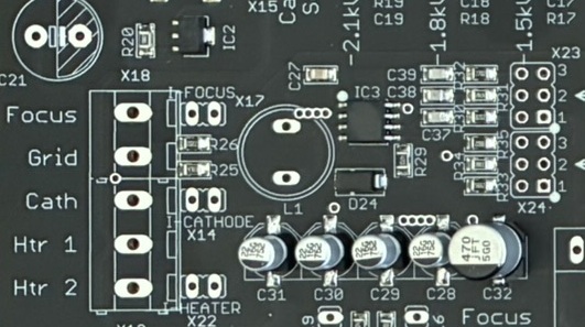
The pattern is worth noting: the discrete choices (which heater voltage, whether PDA is in play, which node the meter watches) are jumpers; the continuous adjustments (bias, focus, accel level, deflection gain and position) are pots. That is the whole user interface — a tube-era-appropriate panel of knobs and links with no firmware between you and the electron beam. The photo above shows this physically: a bank of pots and a field of banana jacks, nothing else.
4.12 Putting it together — the signal-flow summary
To close the loop, here is the whole instrument as one signal-flow, every block traced back to the single 12 V input:
  12 V DC in ──┬─► HEATER converter ─────────────► heater banana (2.5–6.3 V, ≤6 W)
   (2.1mm)     │
               ├─► NEG-RAIL gen ──► [filter] ──► BRIGHTNESS pot ──┬─► g1 banana
               │                                                  ↑  (−5…−120 V)
               │                              Z-axis in ──┤├──────┘  (AC-coupled)
               │
               ├─► ±300 V rails ──► X push-pull ◄──┤├── X in ─────► X plates
               │                └─► Y push-pull ◄──┤├── Y in ─────► Y plates
               │                                   (AC-coupled)   (±300 V diff)
               │
               └─► FLYBACK ─► multiplier ladder ──┬─► a2 tap ──┬─► FOCUS divider ─► a1 banana
                   (custom xfmr)                  │  (≤2.2 kV) └─► a2 banana
                                                  └─► PDA tap ────► PDA banana (≤5.6 kV)

     external DMMs tap: cathode-return current • g1/a1 volts • a2/PDA volts (HV probe)
Every arrow on that diagram started as 12 V DC. The heater rail is stepped down; the grid rail is inverted and filtered; the deflection rails are a moderate boost driven push-pull; and the EHT — the reason the box exists — is flybacked and multiplied up three orders of magnitude to the +2.2 kV and +5.6 kV a CRT’s gun and PDA helix demand. That transformation, from one harmless low-voltage input to the full spread of potentials an electron gun needs, all referenced to one cathode-return node and all set by hand, is the Electrostatic CRT Tester Mark 2.
Vol 5 opens the box for real — the kit tiers, the PCB, the case, and Jeff’s own build. Vol 6 takes these supplies and turns them into a cold-start bring-up-and-measure ritual. Everything both of those volumes do rests on the architecture traced here: know which knob owns which electrode, and know that every one of them is charged from — and traceable back to — a single 12 V rail.
⚠ Safety recap for this volume. Three classes of stored, lethal charge live in this box after power-off: (1) the EHT multiplier ladder at up to +5.6 kV; (2) the ±300 V deflection rails and their AC-coupling caps at the front-panel X/Y jacks; (3) the −120 V grid rail filter cap. None of them self-discharge quickly, because their normal loads (beam current, plate leakage, grid leakage) are all near zero. Bleed every HV node — a2, PDA, X, Y, Z, g1 — to the cathode return before reaching into the neck or handling the input jacks. One-hand rule above ~50 V; EHT-rated leads and a kV-rated bleeder only. Full safety discipline is Vol 8.