Heathkit IP-32 HV Power Supply · Volume 2
Heathkit IP-32 — Vol 2: How It Regulates — The Series-Pass Tube Regulator
Six tubes, six silicon diodes, and two selenium rectifiers turn a raw 600 V bus into a bench-safe, glass-clean 0–400 V rail — with not one transistor in the loop.
⚠ Danger — read before continuing. Every circuit block described in this volume operates at lethal voltage. Raw B+ sits at roughly 600 V DC; the regulated output runs to 400 V DC; the negative reference chain runs to −300 V DC. The filter capacitors hold their charge long after the supply is switched off and unplugged, because the only discharge path is a ~3 mA bleeder (§8, below). None of this volume is a substitute for the shared bench-safety doc — read
_shared/legal_ethics.mdbefore opening the chassis, and see Vol 4 for the full operating-safety procedure.
2.1 The Regulation Philosophy — An All-Tube Loop Wrapped Around a Solid-State Rectifier
Vol 1 introduced the IP-32 as the tube-regulated member of the PS-4→IP-32→IP-17→IP-2717(A)/SP-2717A lineage. This volume is where that claim gets proven at the schematic level. It is worth restating plainly, because the unit’s own parts list makes the mistake easy to fall into: the IP-32 regulates with vacuum tubes, full stop. There is not a single transistor anywhere in the regulation loop, the reference chain, or the control amplifier.
The confusion has an obvious root cause. The main B+ rectifier — the stage that turns the transformer’s AC secondary into a raw DC bus for the pass tubes to work from — is built from silicon diodes in a voltage-doubler arrangement (§5). Silicon rectifiers are a solid-state part, and it is tempting to read “silicon diodes inside” as “solid-state supply.” But a rectifier is not a regulator. Turning AC into rough DC is a completely different job from holding that rough DC at a precise, load-independent, line-independent set point — and that second job, the one that actually earns the word “Regulated” on the front panel, is done entirely by tubes:
Table 1 — The confusion has an obvious root cause. The main B+ rectifier — the stage that turns the transformer's AC secondary into a raw DC bus for the pass tubes to work from — is built from silicon diodes in a voltage-doubler arrangement (§5). Silicon rectifiers are a solid-state part, and it is tempting to read "silicon diodes inside" as "solid-state supply." But a rectifier is not a regulator. Turning AC into rough DC is a completely different job from holding that rough DC at a precise, load-independent, line-independent set point — and that second job, the one that actually earns the word "Regulated" on the front panel, is done entirely by tubes
| Function | Device(s) | Tube or solid-state? |
|---|---|---|
| Series-pass element (the “valve” between raw B+ and the output) | Two 6L6 | Tube |
| Control / error amplifier (compares output to reference, drives the pass tubes) | One 6BH6 | Tube |
| Voltage reference (defines what “regulated” means) | Two 0A2 gas-regulator tubes | Tube |
| Bias-supply rectifier | One 6X4 | Tube |
| B+ rectifier (raw DC only — no regulation function) | 4 silicon diodes, full-wave doubler | Solid-state |
| Screen rectifier (raw DC only — no regulation function) | 2 selenium rectifiers, half-wave | Solid-state (metal-oxide) |
Every device that actually decides what the output voltage will be — the pass element, the amplifier that watches it, and the reference it’s watched against — is a vacuum tube. The two rectifier stages are along for the ride, doing nothing more sophisticated than a doorbell transformer’s rectifier would do: converting AC to unregulated DC so the tube circuitry downstream has something to work with. Get this straight before reading the rest of the volume, because every subsequent section assumes it.
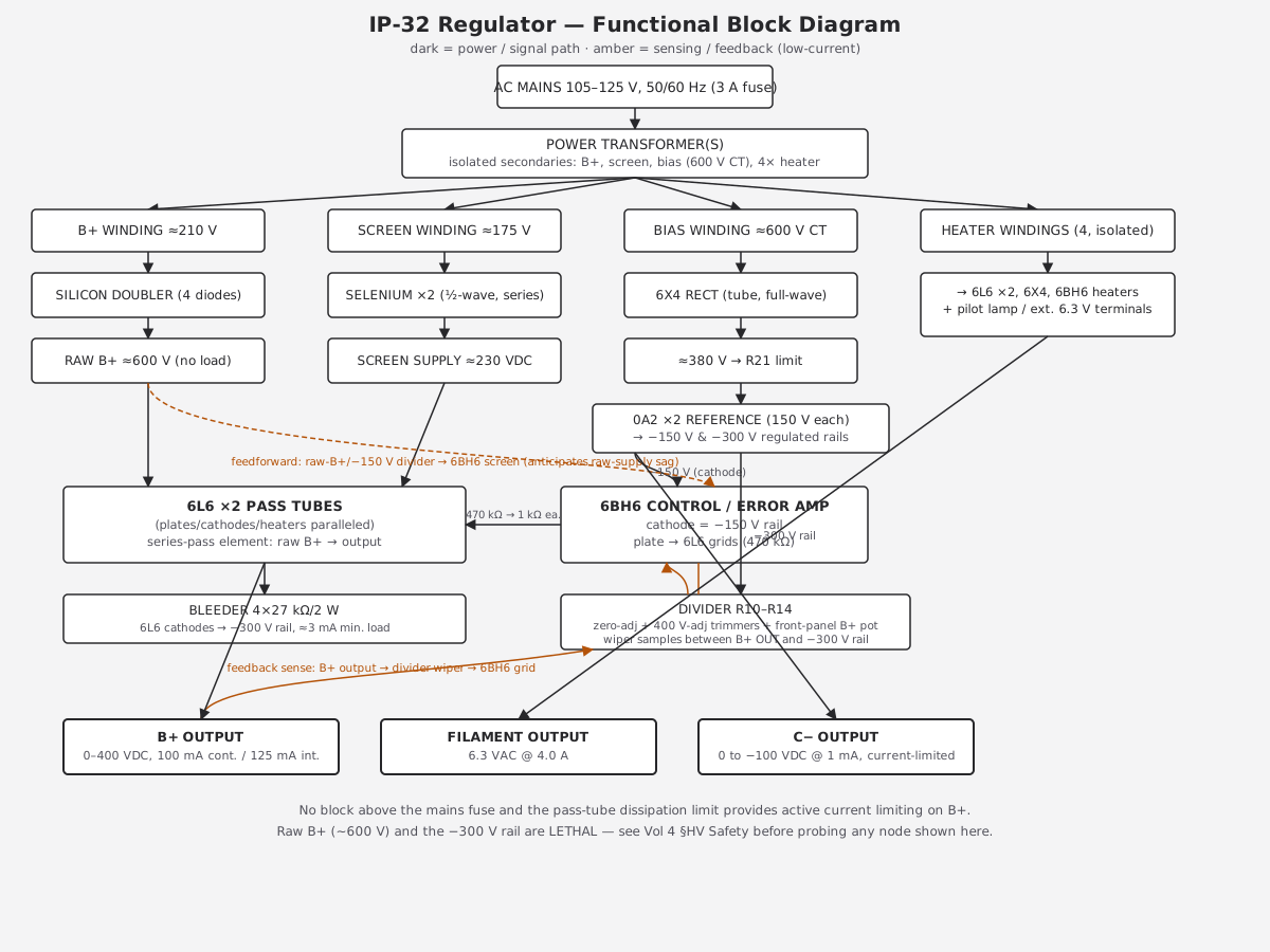
The block diagram below lays out all six functional groups — mains input, the four secondary chains hanging off the power transformer(s), the two active tube stages, and the three front-panel outputs — with the feedback and feedforward paths (amber) distinguished from the power path (dark). Everything in the remaining sections of this volume is a zoomed-in view of one piece of this diagram.
2.2 The Series-Pass Element — Two 6L6 Tubes as a Variable Resistor
2.2.1 The Basic Idea: A Tube as a Rheostat
A series-pass regulator works on a simple principle: put a variable resistance in series between an unregulated (and usually higher) DC bus and the load, then adjust that resistance continuously so the voltage drop across it absorbs exactly the difference between the raw bus and the desired output. Raise the load current or let the raw bus sag, and the pass element’s resistance is trimmed down to compensate; lighten the load or let the raw bus rise, and the pass element’s resistance is trimmed up. The output stays put while everything upstream of the pass element moves around.
A vacuum tube is a natural fit for this job because plate current is a continuous function of grid voltage — there is no discrete “on/off,” only a smooth, controllable conduction curve. Feed the grid a slowly varying control voltage and the tube’s effective plate-to-cathode resistance slides up and down in response. That is exactly what the IP-32’s two 6L6 tubes do, wired as the “valve” between the raw ~600 V B+ bus (§5) and the 0–400 V front-panel output.
2.2.2 Series-Pass vs. Shunt — Why This Topology
Vacuum-tube regulators of this era generally took one of two forms: series-pass, where the regulating element sits in series with the load and drops the difference between raw and regulated voltage, or shunt, where the regulating element sits in parallel with the load and diverts whatever current the load isn’t using, so that a fixed series dropping resistor always sees a constant total current. The IP-32 is unambiguously series-pass — the 6L6 pair sits directly between the raw B+ bus and the output, in series with whatever load is connected.
The trade-off between the two is efficiency versus simplicity of the current-sensing problem, and it explains a fair amount of what shows up elsewhere in this volume. A shunt regulator wastes power continuously (the shunt element burns current the load doesn’t need, all the way down to zero load), but it inherently limits current, because the series dropping resistor caps the total current the whole circuit can ever draw regardless of what the shunt element does. A series-pass regulator like the IP-32’s is far more efficient at partial load — the pass tubes only burn as much power as the difference between raw and set voltage requires — but, as §9 covers, that efficiency comes at the cost of having no inherent current limit at all. The pass element is the only thing standing in the current path, and if something downstream tries to pull more current than the design allows, the pass tubes have no shunt path to bleed off the excess; they simply have to carry it, with only their own dissipation ceiling and the mains fuse as backstops. That single topological choice is the through-line connecting the pass-tube dissipation math in §2.3 to the current-limiting discussion in §9 — they’re the same design trade-off, viewed from two different angles.
2.2.3 Two Tubes, Paralleled
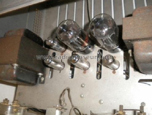
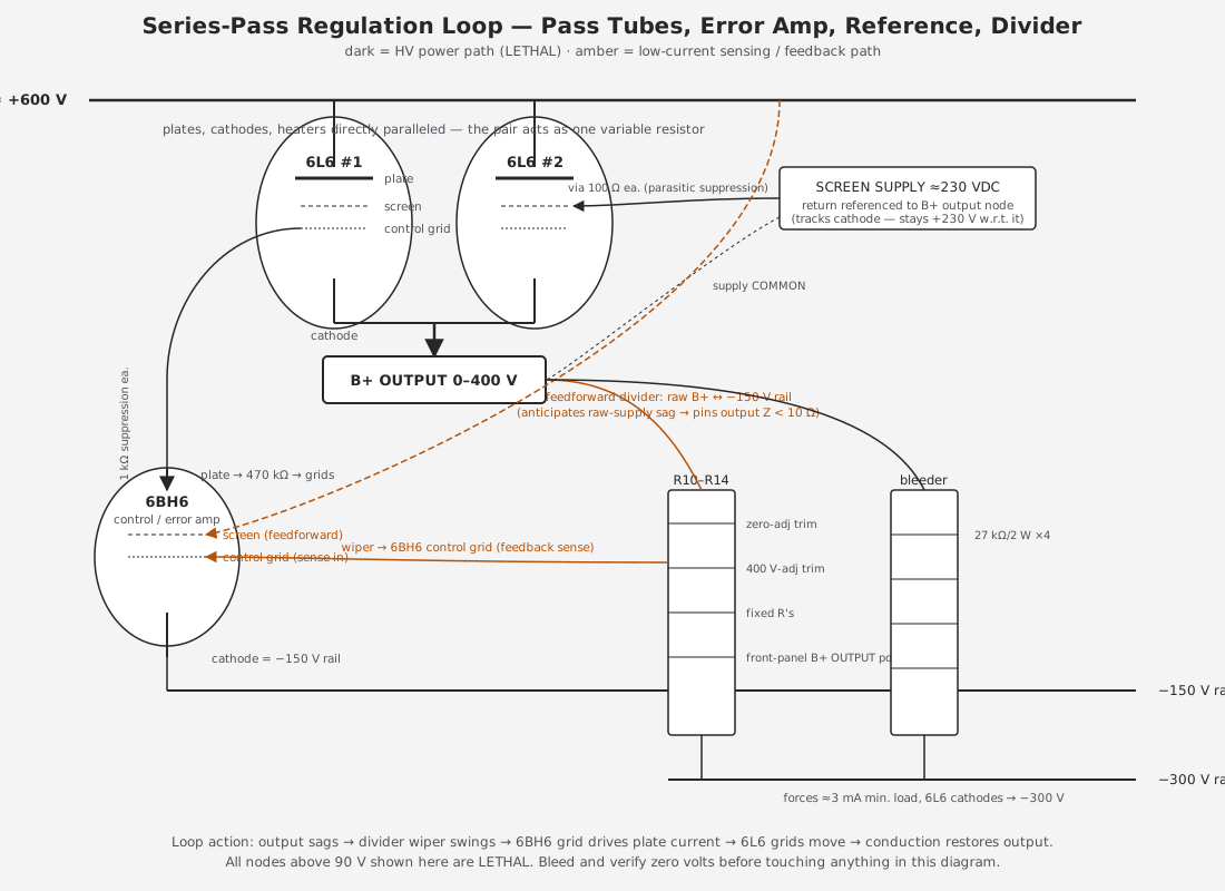
The IP-32 uses two 6L6 tubes rather than one, with plates, cathodes, and heaters directly tied together — electrically, it behaves as a single pass device with twice the current-handling capacity of one 6L6. This is a current-sharing decision, not a voltage-sharing one: both tubes see the same plate-to-cathode voltage at all times (their plates and cathodes are common nodes), so each carries roughly half of whatever total current the pass stage is asked to deliver. At the full 100 mA continuous rating, each 6L6 is carrying on the order of 50 mA — well inside a single 6L6’s comfortable range, and the reason a single-tube design would have needed a much larger, hotter-running power tube to hit the same current spec.
Paralleling pass tubes has a well-known gotcha: if the two tubes don’t have closely matched characteristics, one will hog more of the shared current than the other, running hotter and aging faster while its partner loafs. The IP-32’s paralleled-heater, paralleled-cathode, paralleled-grid, paralleled-plate wiring gives the two tubes no room to disagree about operating point — they are driven by literally the same node at every electrode — so matching is enforced by the topology rather than by hand-selected tube pairs. This is a deliberate simplicity trade Heath made for a kit product: no matched-pair sourcing requirement, no balance trimmers, just “buy two 6L6 tubes and put them in the sockets.”
2.2.4 Plate Dissipation — Where the Watts Go, and the Metal-Can Trap
The pass tubes’ job is to burn off, as heat, whatever voltage the raw B+ bus has left over once the output setting is subtracted. That means the worst-case dissipation condition for the pass tubes is not full output — it’s the combination of low output voltage and high output current, because that’s when the tubes are dropping the largest fraction of the ~600 V raw bus while still passing significant current.
Run the numbers at the extreme: raw B+ ≈ 600 V, output set near 0 V, and the full rated 100 mA continuous still flowing (a legitimate operating point — nothing on the front panel stops you from cranking B+ OUTPUT down to zero while a load pulls full current). The pass-tube pair then has to drop essentially the entire 600 V raw bus while carrying 100 mA:
P(total) = V(drop) × I(load) ≈ 600 V × 0.100 A = 60 W
P(per tube, paralleled 50/50) ≈ 30 W
That arithmetic lands right at the 30 W plate-dissipation rating of a 6L6GC, which is the tube type this circuit needs if it’s going to be run near its rated envelope. A metal-can 6L6 / 6L6GA / 6L6GB, rated closer to 19 W plate dissipation, is comfortably over its limit under that same worst-case condition — and that is exactly the failure mode antique-radio restorers report on IP-32 units built or re-tubed with the older metal-envelope parts: fine at moderate settings, then a slow cook (or an outright short) when someone dials the output low under load. Use 6L6GC pass tubes if the supply is going to see its full rated current at low output-voltage settings; that is not a nostalgia choice, it is a dissipation-margin choice.
⚠ Danger — the pass tubes’ plates sit directly on the raw B+ bus (§5) at roughly 600 V. Even with the supply’s front panel reading a modest output voltage, the plate-to-cathode voltage across the pass tubes can still be hundreds of volts. Never assume a low meter reading means the internal nodes are safe to touch.
2.2.5 Screen and Control-Grid Wiring
Each 6L6’s screen grid is fed from the separate ~230 VDC screen supply (§6) through its own 100 Ω resistor — a classic parasitic-suppression value, there to damp any tendency toward VHF parasitic oscillation in a paralleled-tube stage rather than to do any meaningful voltage dropping. The screen supply itself is worth a second look: its return (common) is referenced to the 6L6 cathode node — i.e., to the B+ output rail itself — rather than to chassis ground, so the screens sit at a fixed +230 V with respect to the cathode no matter where the B+ OUTPUT pot has the output set. That detail matters for the dissipation picture in §2.3: screen dissipation and screen-to-cathode bias stay constant across the whole 0–400 V range, instead of swinging wildly the way they would if the screen supply were referenced to chassis ground while the cathode moved.
Each control grid is fed from the 6BH6 control tube’s plate through its own 1 kΩ suppression resistor — again primarily a stability measure for the paralleled pair, not a significant part of the DC bias network. It is this control-grid node, common to both 6L6 grids, that the error amplifier described in the next section actually drives.
2.3 The Error Amplifier — 6BH6 Control Tube
2.3.1 Role in the Loop
If the two 6L6 tubes are the muscle of the regulator, the 6BH6 is the nervous system. It is a single pentode wired as a DC amplifier whose job is to compare a sample of the actual output voltage against a fixed reference, and turn any difference — however small — into a grid-voltage swing at the 6L6 pass tubes large enough to correct it. This is negative feedback in its most literal form: sag at the output produces a corrective push back toward the set point. The correction is not a discrete, once-a-moment nudge — it’s a continuous analog loop, and it settles far faster than any load transient a bench experiment can throw at it: the same published output impedance figure this dive returns to in §3.3 and §10 (under 10 Ω, holding flat out to 1 MHz) only makes sense if the loop’s own response reaches into that same high-frequency range, not just a few corrections a second.
Per the manual’s circuit description, the 6BH6’s cathode is tied to the regulated −150 V rail (§4) and its plate feeds the 6L6 control grids through a 470 kΩ resistor. Framed as a loop: raise the output above its set point, and the sensing divider’s tap (below) pulls the 6BH6 grid more positive relative to its −150 V cathode, increasing 6BH6 plate current, pulling the plate node (and therefore the 6L6 grids) more negative, reducing 6L6 conduction, and dragging the output back down. Let the output sag, and the same chain runs in reverse. The loop’s whole purpose is to make that correction fast and deep enough that the front-panel meter never has to move to prove it happened.
2.3.2 The Sensing Divider — R10 through R14
The 6BH6’s control grid is driven by the wiper of a resistive divider chain, labeled R10–R14 in the manual, strung between the B+ output node and the regulated −300 V rail (§4). That divider is made up of:
- Two internal trimmer potentiometers — a zero-adjust and a 400 V-adjust — accessible from inside the chassis (Vol 5 covers the calibration procedure for both).
- Fixed resistors setting the overall divider ratio.
- The front-panel B+ OUTPUT potentiometer, which is simply the user-accessible tap point in the same divider chain.
This is the single most important thing to understand about how the front-panel B+ OUTPUT knob actually works: it does not directly control the pass tubes at all. Turning it moves the sensing divider’s set point, which the 6BH6/6L6 loop then chases. The knob sets a target; the loop hits the target. That is also why a fault in this divider chain reads as a calibration fault rather than a dead supply fault — the classic IP-32 gotcha here is a leaky ~0.047 µF coupling capacitor in the 6BH6 control-grid-to-6L6-cathode signal path, which breaks the interaction between the zero-adjust and 400 V-adjust trimmers and makes the output impossible to properly zero or full-scale. See Vol 5 for the fix.
2.3.3 Feedforward — Pinning Output Impedance Near Zero
A pure feedback loop like the one above already gets a regulated supply’s output impedance down substantially, but it has an inherent limitation: it can only react to an error after that error has already appeared at the output. The IP-32 adds a second signal path that does better than react — it anticipates.
The 6BH6’s screen grid is fed not from a fixed supply but from a divider strung between the raw B+ bus and the −150 V rail. Because raw B+ is the least-regulated node in the whole chassis — it sags under heavy pass-tube current draw and dips directly with the AC line — this screen-grid divider gives the 6BH6 a live preview of exactly the kind of disturbance (a raw-supply sag) that the pass tubes are about to have to absorb. Changing the 6BH6’s screen voltage changes its transconductance and plate current before the output divider (§3.2) has had time to show any error at all, so the pass-tube correction starts moving in the right direction essentially in step with the disturbance rather than one loop-delay behind it.
This feedforward path is the specific mechanism behind the IP-32’s published output impedance figure: under 10 Ω from 1 Hz to 1 MHz. For a tube regulator with no active current-limit circuitry and only a passive bleeder for a minimum load (§8–9), sub-10-Ω output impedance across nearly six decades of frequency is a genuinely good result, and it is bought specifically by combining classic feedback (the R10–R14 output divider into the control grid) with feedforward (the raw-B+ divider into the screen grid) rather than by feedback alone.
⚠ Danger — the 6BH6’s cathode sits on the −150 V rail and its screen/grid dividers touch both the raw B+ bus and the −300 V rail. This is a small tube doing a delicate job, but every node around it is at a dangerous potential relative to chassis. Treat the control-amplifier stage with the same discipline as the pass tubes.
2.3.4 Loop Gain, Qualitatively — Why a Small Tube Can Control a Big One
It’s worth pausing on how little signal the 6BH6 actually has to move to control a pair of 6L6 pass tubes carrying up to 100 mA at hundreds of volts. This is the essence of why a series-pass regulator built from tubes works at all, and it’s the same principle that makes op-amp-based solid-state regulators work decades later — only the active devices differ.
The 6L6 pass tubes have substantial transconductance (the ratio of plate-current change to grid-voltage change) — a modest swing at the paralleled control grids produces a large swing in the pass tubes’ conduction, and therefore a large change in the voltage dropped across them. The 6BH6, in turn, only has to develop a modest plate-voltage swing of its own to drive that grid swing through the 470 kΩ/1 kΩ resistor network. And the 6BH6’s own control grid only has to move a tiny fraction of a volt — the signal actually present at the R10–R14 divider wiper when the output strays from its set point — to develop that plate swing, because the 6BH6 itself has healthy voltage gain as a pentode amplifier stage.
Chain those three gain stages together (divider error → 6BH6 grid-to-plate gain → 6L6 grid-to-plate transconductance) and the result is a loop that can correct a meaningful output disturbance from a genuinely tiny error signal at the sensing divider. That’s the entire point of closed-loop regulation: the loop gain does the heavy lifting, not the raw power-handling of any single stage. It’s also why a fault that degrades gain anywhere in that chain — a drifted 6BH6, a degraded coupling capacitor, a mismatched divider resistor — shows up on the bench not as a dead supply but as soft regulation: an output that moves more than it should under load or line changes, without necessarily failing outright. Vol 5’s calibration and fault-finding procedure leans on exactly this behavior to localize a regulation problem to a specific stage.
2.4 The Voltage Reference — Two 0A2 Gas-Regulator Tubes
2.4.1 Gas Regulator Tubes in One Paragraph
A 0A2 is a cold-cathode gas-discharge (voltage-regulator, “VR”) tube: once struck into conduction, the ionized gas between its electrodes maintains a nearly constant voltage drop across a wide range of current, in much the same functional role a zener diode plays in a modern circuit — indeed, the 0A2 is the tube-era ancestor of exactly that function, and it is precisely the part the SP-2717A generation eventually replaced with a stack of ten silicon zener diodes (Vol 6). A 0A2 regulates at a nominal 150 V drop.
2.4.2 Two 0A2s in Series — Building −150 V and −300 V from One Bias Supply
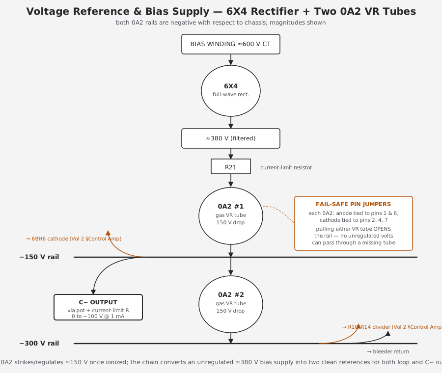
The IP-32 stacks two 0A2 tubes in series, fed from the rectified-and-current-limited bias supply (§7) at roughly 380 V. The first 0A2 drops 150 V from that raw bias node, establishing a clean −150 V rail. The second 0A2 is stacked below the first, dropping another 150 V and establishing a clean −300 V rail. Both rails are regulated by virtue of the 0A2’s flat V-I characteristic — load or line variation upstream of the tubes gets absorbed by the gas discharge’s current swing rather than passed through as a voltage change on either rail.
These two rails do double duty across the chassis:
Table 2 — These two rails do double duty across the chassis
| Rail | Fed by | Used for |
|---|---|---|
| −150 V | 0A2 #1 | 6BH6 cathode reference; feedforward divider return; C− output chain |
| −300 V | 0A2 #2 (stacked below #1) | Top reference for the R10–R14 sensing divider; bleeder return |
Both 0A2 tubes are wear items — as the gas tube ages, its regulation point can drift, which shows up on the bench as an output that no longer tracks the front-panel dial the way it used to, or as a supply that won’t hold calibration through the zero-adjust/400 V-adjust procedure (Vol 5). If regulation performance degrades and the coupling-cap fault (§3.2) has been ruled out, the 0A2 pair is the next suspect.
2.4.3 A Built-In Fail-Safe
Each 0A2 socket uses internal pin jumpers — anode tied to pins 1 and 6, cathode tied to pins 2, 4, and 7 — wired so that pulling a VR tube out of its socket physically opens the rail rather than letting the unregulated bias voltage flow straight through to whatever the tube was regulating. This is a small but genuinely thoughtful piece of kit-era safety engineering: a tube pulled for testing, or simply worked loose in its socket, fails to open circuit rather than failing to full raw voltage. It doesn’t eliminate the hazard of the surrounding nodes, but it does mean a missing 0A2 can’t silently dump ~380 V of unregulated bias onto a rail downstream circuitry (and an operator’s hands) expect to see at −150 V or −300 V.
⚠ Danger — even with the fail-safe jumpering, both 0A2 rails and the raw ~380 V bias node upstream of them are lethal. Gas-regulator tubes can also run visibly hot and glow with a characteristic discharge color when operating normally — don’t mistake normal 0A2 operation for a fault, but don’t touch the glass or the socket while the supply is powered either.
2.5 The B+ Rectifier — Silicon Full-Wave Voltage Doubler
2.5.1 Why a Doubler
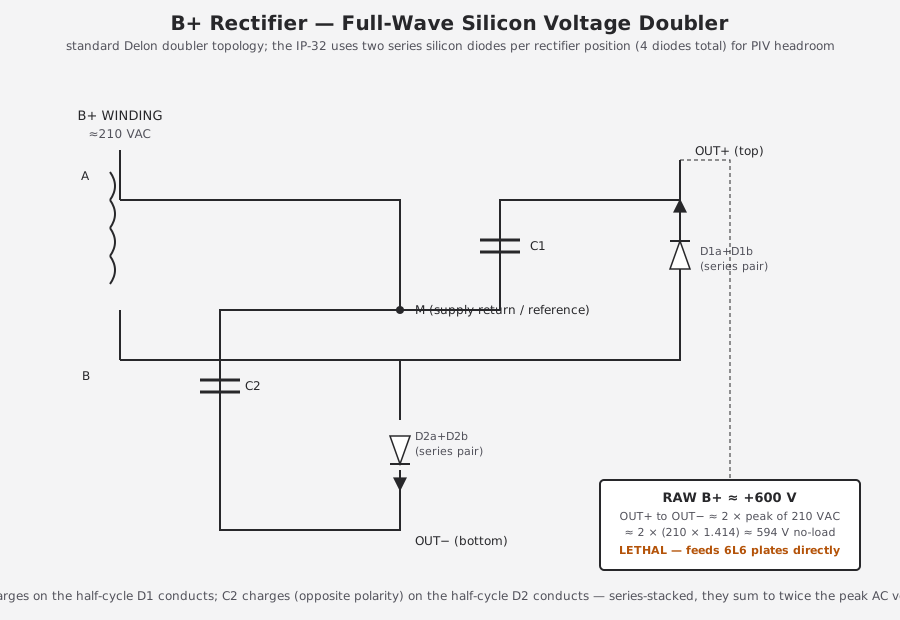
The IP-32 needs a raw DC bus comfortably above its highest regulated output (400 V) so the pass tubes always have headroom to drop across, even at full output and full load. Rather than spec a transformer secondary that swings all the way up to that raw-bus voltage directly (a heavier, more expensive winding), the design uses a more modest ≈210 VAC secondary and doubles it with a rectifier topology instead of a transformer turns ratio. A full-wave voltage-doubler circuit — the classic Delon arrangement — takes an AC source and, using two rectifier positions and two capacitors, produces a DC output at roughly twice the AC input’s peak voltage:
V(out, no load) ≈ 2 × V(rms) × √2
                 ≈ 2 × 210 V × 1.414
                 ≈ 594 V
That arithmetic lands right on the manual’s quoted ≈600 V raw B+ no-load figure, which is a satisfying sanity check that the ≈210 V winding figure and the ≈600 V raw-bus figure are self-consistent (both individually confirmed against the manual and Eckweiler’s circuit description).
2.5.2 Topology — Two Rectifier Positions, Four Diodes
A basic Delon doubler needs just two rectifier positions (commonly drawn as two diodes) and two capacitors. The IP-32’s B+ doubler is described in the manual as using two series pairs of silicon diodes — four diodes total — rather than a single diode per position. That doubling-up is a PIV (peak inverse voltage) headroom decision: with a raw bus in the 600 V neighborhood, a single low-cost silicon rectifier of the era might not carry enough reverse-voltage rating on its own to survive the full swing safely, so the design puts two diodes in series at each rectifier position to split that reverse-voltage stress across two junctions instead of one. Functionally it is still a two-position doubler; each “position” just happens to be built from two diodes instead of one.
The two filter capacitors sit in series across the doubler’s output, each charged to roughly one AC peak (≈300 V) on alternating half-cycles, so that their series sum delivers the full ≈600 V raw bus. This is also why the doubler’s filter/reservoir capacitors are among the highest-voltage-rated parts in the whole chassis and are a first-look item on any recap (Vol 5) — reported original values are 70 µF at 350 V for the main filter can, with 40 µF and 20 µF cans elsewhere in the supply; treat those specific values as a starting point to verify against the manual’s parts list before ordering replacements, since the full cap-by-cap schematic listing was not exhaustively re-transcribed for this dive.
⚠ Danger — the doubler’s output capacitors are the largest reservoir of stored energy in the entire chassis, sitting at roughly 600 V, and they are what the pass tubes’ plates connect to directly. The bleeder (§8) only pulls a few milliamps through them — they can hold a dangerous charge for a long time after the supply is unplugged. Always manually discharge every electrolytic through a resistor before working inside the chassis, and verify zero volts with a meter before touching anything.
2.5.3 “Solid-State” Only Describes Half the Story
It’s worth returning to the framing question one more time now that the doubler has been laid out in full. Yes — this stage genuinely is solid-state: four silicon diodes, no tubes, no moving parts in the rectification itself. But this stage also does not regulate anything. It has no feedback, no reference, no error correction; it simply turns AC into a lumpy, load-dependent, line-dependent raw DC voltage and hands that raw voltage off to the tube regulator described in §2–4 to actually hold steady. Calling the supply “solid-state regulated” because this one rectifier stage happens to use silicon diodes is the same category error as calling a car “solar powered” because its dashboard clock has a photovoltaic backup battery. The regulation — the entire reason the front panel says “REGULATED” — is 100% vacuum-tube work.
2.6 The Screen Supply — Selenium Half-Wave Rectifier
The 6L6 pass tubes’ screens need their own supply, separate from the raw B+ bus the plates sit on, because (as §2.4 covered) the screen supply’s return floats with the cathode/output node rather than chassis ground. That supply is built from a 175 V transformer winding, half-wave rectified by two selenium rectifiers in series, and filtered down to roughly 230 VDC.
Two things about this stage are worth flagging for anyone servicing the unit:
- Half-wave, not full-wave. Unlike the B+ doubler (full-wave, §5) and the bias supply’s 6X4 (full-wave, §7), the screen supply only rectifies one half of each AC cycle. That’s a reasonable design economy given the screen supply doesn’t need to source much current — the 6L6 screens draw comparatively little compared to the plate current running through the pass tubes — but it does mean the screen supply’s ripple content, before filtering, is inherently rougher than the other two DC stages.
- Selenium rectifiers are a known wear item. Selenium rectifiers age by gradually increasing forward voltage drop and can eventually fail outright, sometimes with the characteristic acrid smell selenium rectifiers are notorious for when they finally let go. Restorers commonly replace the pair with modern silicon diodes plus a series resistor, sized to make up for silicon’s much lower forward drop compared to the selenium stack, so the resulting DC voltage still lands near the original ≈230 V design point. See Vol 5 for the swap procedure and resistor-sizing approach.
⚠ Danger — selenium rectifiers that have begun to fail can run hot and, per general vintage-electronics handling guidance, selenium compounds are best treated as a material to avoid breathing fumes from if a unit is powered up with a badly degraded rectifier. If a selenium rectifier shows physical damage (bulging, discoloration, powdery residue), replace it before re-powering the supply rather than testing through it.
2.7 The Bias / Negative Supply — 6X4 Tube Rectifier
The negative (bias/reference) chain starts from its own ≈600 V center-tapped winding, separate from both the B+ winding and the screen winding. That winding is full-wave rectified by the 6X4 — a small dual-diode tube built specifically for this kind of rectifier duty — yielding roughly 380 V after filtering. From there, R21 current-limits the feed before it reaches the two-stage 0A2 reference chain described in §4, which is the stage that actually turns this rough ≈380 V into the clean regulated −150 V and −300 V rails the rest of the supply depends on.
Two design choices are worth calling out here:
- A dedicated rectifier tube, not a shared one. The bias supply gets its own 6X4 rather than borrowing rectification from anywhere else in the chassis. That keeps the bias chain’s ripple and loading behavior independent of what the B+ side is doing — a practical necessity given how much the bias rails feed into the sensitive control-amplifier stage (§3), which would be a poor place to let B+-side ripple leak in.
- R21 does the current-limiting, not the 0A2s. The 0A2 tubes regulate voltage; they don’t inherently limit current on their own upstream side. R21’s job is to keep the 6X4’s output from over-driving the 0A2 chain under any load condition the bias/reference circuitry can present, protecting both the 6X4 and the 0A2 pair.
The 6X4’s own heater draws about 0.6 A off one of the four isolated heater windings described next — small next to the 6L6 pair’s combined 2 A, but isolated for the same reason every heater winding in this chassis is isolated: the cathodes it’s heating float at high potential, and a heater winding shared with a grounded reference would bridge that isolation.
2.8 Heater Power — Four Isolated Windings for Floating Cathodes
It’s easy to treat filament/heater power as an afterthought next to the HV story, but the IP-32’s heater arrangement is itself a direct consequence of the regulation topology described above. Because the 6L6 pass tubes’ cathodes sit at the output voltage (0–400 V, moving with the front-panel dial) and the 6BH6’s cathode sits at −150 V, none of these tubes can share a single grounded heater winding the way a simple radio chassis might. Each floating cathode needs its heater supply isolated (and, per the manual, bonded to its own tube’s cathode on one side) so the heater-to-cathode voltage rating of the tube isn’t exceeded and so heater current doesn’t find an unwanted path back through chassis ground.
The IP-32 solves this with a separate heater transformer carrying four isolated windings:
Table 3 — The IP-32 solves this with a separate heater transformer carrying four isolated windings
| Winding | Current rating | Feeds |
|---|---|---|
| Winding 1 | 2.0 A | Both 6L6 pass tubes (paralleled heaters) |
| Winding 2 | 0.6 A | 6X4 bias rectifier tube |
| Winding 3 | 0.15 A | 6BH6 control amplifier |
| Winding 4 | 4.15 A | Pilot lamp + the front-panel external 6.3 VAC filament terminals |
Note that the front-panel filament output (6.3 VAC @ 4.0 A, the spec quoted throughout this dive) is drawn from the same winding that lights the pilot lamp — that winding’s 4.15 A rating gives headroom above the panel’s rated 4.0 A output for the pilot lamp’s own draw.
2.9 The Bleeder — Minimum Load for Loop Stability
2.9.1 Why a Series-Pass Regulator Needs a Minimum Load at All
A series-pass regulator’s ability to raise the output when it sags is limited only by how hard the control loop can drive the pass tubes into heavier conduction — there’s essentially no ceiling on that within the tube’s rating. But its ability to lower the output when the load is light (or absent) is limited by how far the pass tubes can be driven toward cutoff, and a real tube never reaches a perfectly clean, zero-leakage cutoff. At very light external load, if the loop tried to hold a low output purely by throttling the pass tubes toward cutoff, small leakage currents and the nonlinear behavior near cutoff can leave the loop without a clean, well-behaved point to regulate around — the classic “regulator loses control at no load” failure mode common to series-pass designs of this era.
The fix is to guarantee the pass tubes are never asked to sit near cutoff in normal operation, by forcing a modest current to flow through them at all times regardless of what the external load is doing.
2.9.2 The Bleeder Itself
The IP-32 does this with four 27 kΩ, 2 W resistors wired in series, connected from the 6L6 cathodes (the B+ output node) to the −300 V rail. Because the bleeder’s far end sits at −300 V rather than chassis ground, the total voltage across the four-resistor string is the B+ output setting plus 300 V — meaning the bleeder draws current across the entire 0–400 V range, even when the front panel is dialed all the way down to zero. Four 27 kΩ resistors in series total 108 kΩ; across a worst-case ~300 V minimum (output at 0 V, bleeder string spanning 0 V to −300 V) that works out to roughly 3 mA — matching the manual’s quoted minimum-load figure.
That 3 mA is deliberately small — small enough that it doesn’t meaningfully cut into the 100 mA rated output capacity available to an actual external load — but it is exactly enough to keep the pass tubes biased into a well-controlled part of their conduction curve at all times, which is what “keeps the pass tubes in control at no load” means in practice.
2.9.3 The Same 3 mA Explains Why Capacitors Stay Charged
This bleeder does double duty as the only built-in discharge path for the doubler’s filter capacitors (§5) once the supply is switched off. A 3 mA bleed rate is a design point chosen for regulation stability, not for a fast, safe power-down — at that current, a 70 µF capacitor charged to 600 V takes a genuinely long time to bleed down to a safe level on its own. This is precisely why the bench-safety procedure in Vol 4 and the shared bench-safety doc both insist on manually discharging the filter capacitors through a resistor before reaching inside the chassis, rather than trusting the bleeder (or elapsed time since unplugging) to have done the job.
⚠ Danger — never assume “it’s been unplugged for a while” means the filter caps are safe. A 3 mA bleeder on a 70 µF/350 V-class capacitor bank charged to 600 V is not a fast discharge path. Verify zero volts with a meter, and manually discharge through a resistor first, every time.
2.10 Why There’s No Active B+ Current Limit
A modern bench supply almost always has some form of active current limiting or foldback on its main output — a circuit that senses output current directly and clamps the pass element’s conduction before a fault condition can do damage. The IP-32 has none of that on the B+ output. It’s worth being explicit about this, because it’s a real and consequential design characteristic, not an oversight this dive is glossing over.
What the B+ output actually has, protecting it against overcurrent, is:
- The rear-panel 3 A mains fuse — a blunt, whole-supply-level protection device that trips on gross fault conditions (a shorted output, a shorted rectifier, a failed pass tube dragging heavy current) but does nothing to protect against a sustained moderate overcurrent condition that stays under 3 A at the primary while still cooking something downstream.
- The pass tubes’ own plate dissipation limit — as worked out in §2.3, the 6L6 pair (specifically, 6L6GC-rated at 30 W each) has a hard thermal ceiling. If an external load pulls sustained heavy current at a low output-voltage setting, the pass tubes are the thing standing between “the supply works as designed” and “the pass tubes cook themselves,” and nothing in the circuit intervenes to stop that from happening short of the tubes actually failing.
There is a second, quieter consequence worth flagging: the antique-radio-forum service consensus on this design is that the main power transformer is itself somewhat under-rated for sustained heavy-overcurrent conditions, meaning a prolonged fault that the 3 A fuse doesn’t clear promptly can stress the transformer primary — and transformers for a 1960s Heathkit lab supply are not a part that’s easy to source new. Practically, that means the operator’s own discipline (don’t run the supply into a dead short and walk away; don’t lean on the output at low-voltage/high-current settings for extended periods) is doing real protective work that a modern current-limited bench supply would do automatically. Vol 4 covers the operating procedure that keeps this design characteristic from becoming a problem in practice; Vol 5 covers what to check on the transformer and fuse during a refurbish.
Contrast this with the C− (bias) output, which is internally current-limited (§4, and see Vol 3 for the exact bias-chain component that does it) — which is also why the bias output is rated at only 1 mA and doesn’t get a current meter on the front panel at all: there’s no meaningful current range to display, and the limiting is already baked into the circuit rather than left to the operator.
2.11 Load & Line Regulation — What the Published Numbers Actually Mean
Vol 1 quoted the IP-32’s headline regulation figures without dwelling on them. Having walked the whole loop, it’s worth coming back to those numbers and reading them the way a bench engineer should — as a statement about this specific loop’s gain and reference stability, not as marketing copy.
Table 4 — Load & Line Regulation — What the Published Numbers Actually Mean
| Spec | Value | What it’s really saying |
|---|---|---|
| Load regulation | ±1 %, no-load to full-load, 100–400 VDC | At 400 V output, the loop holds the set point to within about ±4 V as the load swings from nothing to the full rated 100 mA. That’s the R10–R14 feedback loop (§3.2) doing its job across the full current range the pass tubes are rated for. |
| Line regulation | ±0.5 V output change per 10 V line change | A 105–125 V mains wander (the supply’s full rated input range, §Vol 1) is well over 10 V — but because the raw B+ bus, screen supply, and reference chain all move together and the feedforward path (§3.3) is watching the raw bus directly, the output barely notices. |
| Ripple, jitter & noise | < 10 mV | This is the residual AC content the doubler’s filter caps and the loop’s own dynamic response fail to remove entirely. Because the doubler is only full-wave (not, say, a multi-stage RC filter), most of this figure’s headroom is bought by loop gain rather than brute-force filtering. |
| Output impedance | < 10 Ω, 1 Hz – 1 MHz | The figure directly attributable to the feedforward path (§3.3) doing work a feedback-only loop couldn’t match at higher frequencies, where the loop’s own reaction time starts to lag the disturbance. |
None of these four numbers describes an isolated component — each is the emergent behavior of the whole loop from §2 through §8 working together. That’s worth internalizing before troubleshooting a “regulation seems soft” complaint on a real unit: the fault could be sitting anywhere in that chain, and diagnosing it means checking the loop’s building blocks one at a time (pass-tube bias, 6BH6 operating point, 0A2 rail voltages, divider resistor values) rather than assuming a single obviously-bad part will explain a general softening of these specs. Vol 5 has the bench procedure for exactly that kind of methodical check.
⚠ Danger — verifying any of these specs on the bench means probing live nodes at hundreds of volts with the supply powered and delivering current into a load. Use properly rated HV probes, keep one hand in your pocket, and never probe blind — know what voltage you expect at a test point before you touch it there. See Vol 4 for the full live-measurement procedure.
2.12 Putting the Loop Together — A Full Signal-Flow Walkthrough
With every block now covered individually, it’s worth walking the whole loop start to finish, the way a fault-finding session on the bench actually has to think about it.
- AC mains enters through the rear-panel 3 A fuse and drives the power transformer(s), which present four isolated secondaries: the B+ winding (≈210 V), the screen winding (≈175 V), the bias winding (≈600 V CT), and the heater windings (four separate, §6).
- The B+ winding feeds the silicon voltage doubler (§5), producing a raw B+ bus of roughly 600 V with no active regulation of its own — this bus sags under load and moves with the AC line, and it is precisely that raw, unregulated behavior the rest of the loop exists to hide from the output.
- The screen winding feeds the selenium half-wave rectifier (§6), producing roughly 230 VDC, referenced not to chassis ground but to the 6L6 cathode/output node, so the pass tubes’ screens always sit a fixed 230 V above their own cathodes.
- The bias winding feeds the 6X4 full-wave rectifier (§7), producing roughly 380 V, current-limited by R21, and regulated down by the two-stage 0A2 chain (§4) into clean −150 V and −300 V rails.
- The raw B+ bus connects directly to the 6L6 pass tubes’ plates. The pass tubes’ cathodes, tied together, are the B+ output node.
- The B+ output node is sampled by the R10–R14 divider (§3.2), whose wiper — set by the front-panel B+ OUTPUT pot plus the two internal trimmers — drives the 6BH6 control grid.
- The raw B+ bus is also sampled, separately, by a feedforward divider (§3.3) that drives the 6BH6 screen grid, giving the amplifier an early look at raw-supply sag before it reaches the output.
- The 6BH6’s cathode sits on the regulated −150 V rail, giving the whole amplifier stage a stable reference to compare against.
- The 6BH6’s plate, through 470 kΩ, drives both 6L6 control grids (through their individual 1 kΩ suppression resistors) — closing the loop: any deviation the 6BH6 detects turns directly into a correction at the pass tubes.
- The bleeder (§8), running from the B+ output node to the −300 V rail, guarantees the pass tubes always carry at least ≈3 mA, so the loop never has to operate near cutoff even with no external load connected.
- The corrected, regulated B+ output appears on the front-panel binding posts at 0–400 VDC, 100 mA continuous (125 mA intermittent) — the number the whole chapter has been building toward, and the number Vol 3 picks up to cover the metering and front-panel hardware that lets the operator actually see and set it.
2.12.1 Quick-Reference — Every Node Named in This Volume
The table below collects every rail and node discussed above into one place, ordered roughly from raw/unregulated to fully regulated. It doubles as a bench cheat-sheet for anyone tracing the loop with a meter — but every voltage in it is a chassis-referenced DC (or, where noted, AC) figure at a lethal potential, and several are negative with respect to chassis rather than positive.
Table 5 — Quick-Reference — Every Node Named in This Volume
| Node | Approx. voltage | Regulated? | Where it’s driven from |
|---|---|---|---|
| B+ winding (AC) | ≈210 VAC | No | Power transformer secondary |
| Screen winding (AC) | ≈175 VAC | No | Power transformer secondary |
| Bias winding (AC, CT) | ≈600 VAC CT | No | Power transformer secondary |
| Raw B+ bus | ≈+600 VDC no-load | No | Silicon voltage doubler (§5) |
| Screen supply | ≈+230 VDC (w.r.t. cathode) | No (but floats with cathode) | Selenium half-wave rectifier (§6) |
| Bias raw node (post-6X4, pre-R21) | ≈+380 VDC magnitude, negative rail | No | 6X4 full-wave rectifier (§7) |
| −150 V rail | −150 VDC | Yes (0A2 #1) | Two-stage 0A2 chain (§4) |
| −300 V rail | −300 VDC | Yes (0A2 #2, stacked) | Two-stage 0A2 chain (§4) |
| B+ output (6L6 cathodes) | 0 to +400 VDC, front-panel set | Yes (closed loop) | 6L6 pass-tube pair (§2), driven by the full loop |
| C− output | 0 to −100 VDC | Yes (internally current-limited) | −150 V rail through C− pot + limit R |
| Filament output | 6.3 VAC | No (transformer-derived only) | Dedicated heater winding (§6) |
Vol 3 covers the physical chassis this loop lives in — the specific hardware, connectors, and metering circuit that surrounds everything described here, including exactly where on the chassis each of these nodes can be safely reached with a meter probe. Vol 4 covers the operating procedure and the full HV safety discipline for working with a supply built exactly this way. Vol 5 covers refurbishing this specific loop — the recap values, the selenium-to-silicon screen-rectifier swap, the 6L6GC dissipation consideration, and the leaky-coupling-cap fault that breaks the zero/400 V calibration described in §3.2. Vol 6 sets this whole regulation scheme side by side with the SP-2717A’s solid-state-reference successor, where the two 0A2 tubes in §4 give way to a stack of ten silicon zener diodes doing the identical reference job — the one part of this generational pair that genuinely did go solid-state.
Sources
- Heathkit IP-32 assembly & operation manual (scans): archive.org — https://archive.org/details/Heathkit_IP-32_HV_Power_Supply ; vintage-radio.info — https://www.vintage-radio.info/download.php?id=212 ; elektrotanya — https://elektrotanya.com/heathkit_ip-32_regulated_power_supply.pdf/download.html ; Berkeley (image-only scan) — https://experimentationlab.berkeley.edu/sites/default/files/NMR/Equipment/Heathkit%20IP-32_Regulated%20Power%20Supply_Manual.pdf
- Bob Eckweiler (AF6C), “Heathkit of the Month #67 — IP-32 Bench HV Power Supply,” OCARC RF newsletter, Aug 2015 — https://www.w6ze.org/Heathkit/Heathkit_067_IP32.pdf
- radiomuseum.org, Heathkit IP-32 listing (dates, tube complement, dimensions, price) — https://www.radiomuseum.org/r/heath_regulated_power_supply_ip_5.html
- pudar.net, “Heathkit IP-32 Restoration” (selenium/silicon screen-rectifier swap, recap notes) — https://pudar.net/heathkit-ip-32-restoration/
- Antique Radio Forums, IP-32 repair thread (leaky coupling capacitor, 6L6GC dissipation, transformer under-rating) — https://antiqueradios.com/forums/viewtopic.php?t=440
- diyAudio, IP-32 regulated supply thread — https://www.diyaudio.com/community/threads/heathkit-ip-32-regulated-supply.360274/
- Chuck Penson, Heathkit Test Equipment Products (styling/production-date reference, as cited by Eckweiler)