Heathkit SP-2717A HVPS · Volume 2
Heathkit SP-2717A — Vol 2: How It Regulates — The Series-Pass Tube Regulator
Two 6L6GC beam-power tubes act as a grid-controlled variable resistor between a 600 V raw bus and a 400 V regulated output, and a lone 6AU6 pentode watches the whole show against a stack of ten zener diodes.
2.1 Overview — The Regulation Loop at a Glance
Vol 1 covers what the SP-2717A does: 0–400 V DC B+ at up to 100 mA continuous (125 mA intermittent), 0 to −100 V DC bias at 1 mA, and a filament tap, all dialed from the front panel. This volume covers how — the circuit that turns a crude, unregulated ~600 V DC bus into a load- independent, line-independent 400 V rail with under 10 Ω of output impedance from DC to 1 MHz.
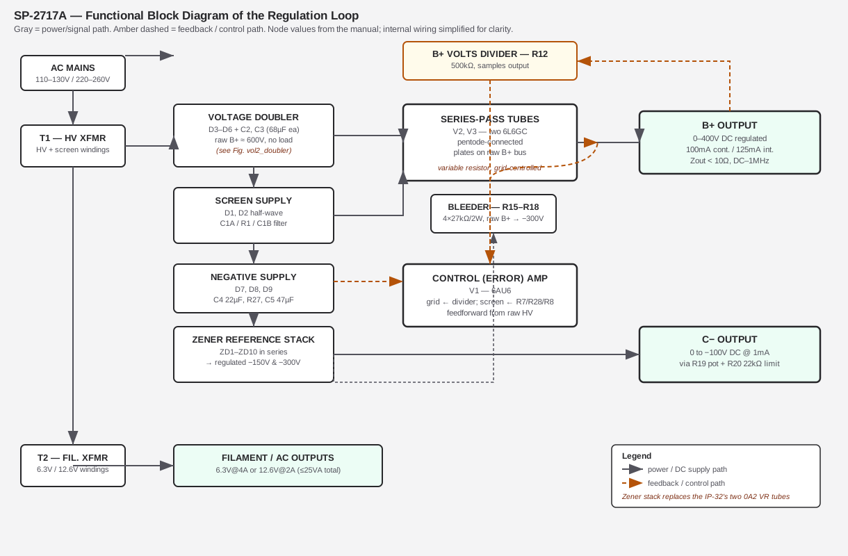
The short version: two 6L6GC beam-power tubes sit in series between the raw high-voltage bus and the B+ output post, acting as a voltage-controlled variable resistor. A third tube, a 6AU6, watches a sample of the output, compares it to a fixed reference, and continuously adjusts the grid voltage on the two 6L6GCs to hold the output constant as load current and line voltage swing. The reference that the 6AU6 compares against is not a pair of glowing 0A2 gas-regulator tubes — that was the IP-32’s generation (Vol 6 covers the full lineage) — it is a series stack of ten silicon zener diodes, ZD1 through ZD10, developing regulated −150 V and −300 V rails from an all-silicon rectifier chain. Every rectifier in the SP-2717A, including the raw B+ supply itself, is silicon. No tube ever rectifies AC to DC in this instrument; tubes here do exactly one job — series-pass control — and diodes do everything else.
That split is the entire story of this volume, and it is worth stating plainly because it resolves an apparent contradiction in how this instrument gets described casually: the SP-2717A is not “tube regulated” in the sense of an all-tube supply, and it is not “solid-state regulated” in the sense of a transistor pass element. It is a hybrid — a tube series-pass regulator with a solid-state rectifier and reference. The pass element that actually drops the volts and dissipates the watts is, and remains, a pair of vacuum tubes.
⚠ Danger — read before opening the chassis. Every circuit described in this volume operates at lethal voltages. The raw B+ bus sits at roughly 600 V DC with respect to common; the reference stack develops −150 V and −300 V rails; the regulated B+ output itself reaches 400 V DC at up to 125 mA. The filter capacitors hold their charge long after the unit is switched off and unplugged, because the only discharge path — the bleeder — is a minimum-load resistor chain, not a fast-discharge circuit (see § “The Bleeder,” below). Treat every internal node as live until you have personally verified it with a meter. Vol 4 covers the full operating and safety procedure; the hub-wide HV/mains discipline rules are in the shared legal & ethics notes — read them before you touch a probe to this chassis.
2.1.1 The basic idea: a variable resistor under feedback control
Strip away the tube envelopes and diode symbols and a series-pass regulator is a simple idea. Put a controllable resistance in series between an unregulated (and higher) input voltage and the load. Continuously measure the output. If it starts to sag — because the load pulled more current, or the line voltage dipped — reduce that series resistance so more current gets through and the output climbs back up. If the output starts to rise, increase the resistance. Do this fast enough, and with enough gain in the measuring/correcting loop, and the output holds essentially constant regardless of what the load or the line does.
A vacuum tube is a natural fit for the “controllable resistance” role: its plate-to-cathode resistance is a function of its grid voltage, and that relationship is smooth, continuous, and — critically for a supply that has to survive a fault — self-limiting in a way a raw switch is not. The SP-2717A uses two 6L6GC beam-power pentodes in parallel for this job (§2 below), driven by a 6AU6 pentode wired as a DC error amplifier (§3), referenced against the ten-zener stack (§4). Closing that loop is the subject of §5.
2.1.2 Why two generations, one circuit family
The IP-32 (1962–67), the direct ancestor three generations back, solves the same problem with the same pass-tube topology — two tubes, series-pass, driven by a control amplifier — but built its reference from two 0A2 gas voltage-regulator tubes and rectified everything, including the bias supply, through a mix of silicon diodes, two selenium rectifiers, and a 6X4 tube rectifier. Both instruments deliver the identical 0–400 V / 100 mA (125 mA intermittent) B+ spec — this is not a low-current/high-current pair, whatever a casual glance at “SP” vs “IP” and a twenty-year gap might suggest (Vol 6 has the full comparison table). What changed between 1962 and 1982 is entirely inside the rectifier and reference circuitry: gas tubes and selenium plates gave way to zener stacks and silicon junctions, while the fundamental job — a tube variable resistor under a tube error amplifier’s control — stayed exactly the same. This volume is the SP-2717A half of that story; the IP-32 project covers its own generation in the same depth.
2.1.3 Why the pass element never went solid-state
It is worth pausing on the fact that the 1982 redesign modernized the rectifier and the reference but left the actual series-pass job — the part carrying the most current at the widest voltage swing — on vacuum tubes. That is not an oversight or a case of Heath being slow to adopt transistors; by 1982 solid-state series-pass regulators were routine at low voltages. The SP-2717A’s pass element, though, has to sit in series with a bus around 600 V and block essentially that entire voltage at the low end of the B+ dial while still being able to pass 100 mA — a combination of high blocking voltage and moderate current that put it well outside what an ordinary, inexpensive power transistor of that era could do safely. Purpose-built high-voltage power transistors existed, but at meaningfully higher cost and lower design familiarity than a pair of 6L6GC beam-power tubes, which were (and remain) a cheap, extremely well-characterized, mass-produced device with exactly the plate-voltage headroom this job needs, decades of application history in exactly this kind of series-regulator role, and a benign overload behavior — a tube driven into excessive dissipation degrades gradually (shortened life, eventual failure) rather than failing instantly and catastrophically the way an overstressed semiconductor junction typically does. For an instrument whose whole purpose is sitting on a bench absorbing whatever a breadboarded tube circuit under test throws back at it, that gradual-failure characteristic is a feature, not a limitation. The rectifier and reference stages, by contrast, never see anything like 600 V across a single silicon junction and benefit straightforwardly from silicon’s lower cost, higher reliability, and total absence of a warm-up period — which is exactly the split the 1982 redesign made.
2.2 The Series-Pass Element — Two 6L6GC Pentodes
2.2.1 Designators and role
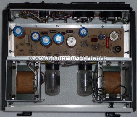
The manual’s Tube and Diode Complement table names the two series-pass tubes V2 and V3, both type 6L6GC (Heath part 411-8). They sit electrically in parallel: both plates tie to the raw B+ bus coming out of the voltage doubler (§6), both cathodes tie together at the regulated B+ output node, and both control grids are driven from the same point in the error-amplifier circuit through individual parasitic-suppressor resistors R4 and R5. Electrically, two paralleled 6L6GCs behave as one larger pass device — halving the plate current, and therefore the plate dissipation, that any single tube has to carry for a given B+ load. At 100 mA continuous B+ current split across two tubes, each 6L6GC only has to handle roughly half the load current, which is a meaningful margin against the tube’s rated plate dissipation when it is also dropping several hundred volts.
2.2.2 Pentode, not triode: the low-dropout argument
The manual is explicit about why the 6L6GC is run as a pentode here rather than strapped as a triode (tying screen to plate, a common trick in audio output stages): a pentode drops less voltage across itself for a given plate current than the same tube triode-connected, which is exactly the property a wide-range series regulator wants. A series-pass element with a large minimum voltage drop wastes headroom — it eats into how close the output can be driven to the raw supply rail before the regulator runs out of control range. Running the 6L6GCs as true pentodes, with their own dedicated screen-grid supply (§7) independent of the plate circuit, keeps that minimum drop low and preserves usable regulation range across the full 0–400 V dial sweep against a raw bus sitting around 600 V.
2.2.3 The pass tube as a physical object
The 6L6GC is a beam-power pentode, descended from the original 6L6 metal-envelope tube of the 1930s, long a workhorse of audio output stages and — as here — regulator pass elements. It is not a small tube: expect it to run warm to the touch in normal operation, because dissipating watts as heat is literally its job in this circuit; that is the price of a purely resistive (as opposed to switch-mode) regulator topology.
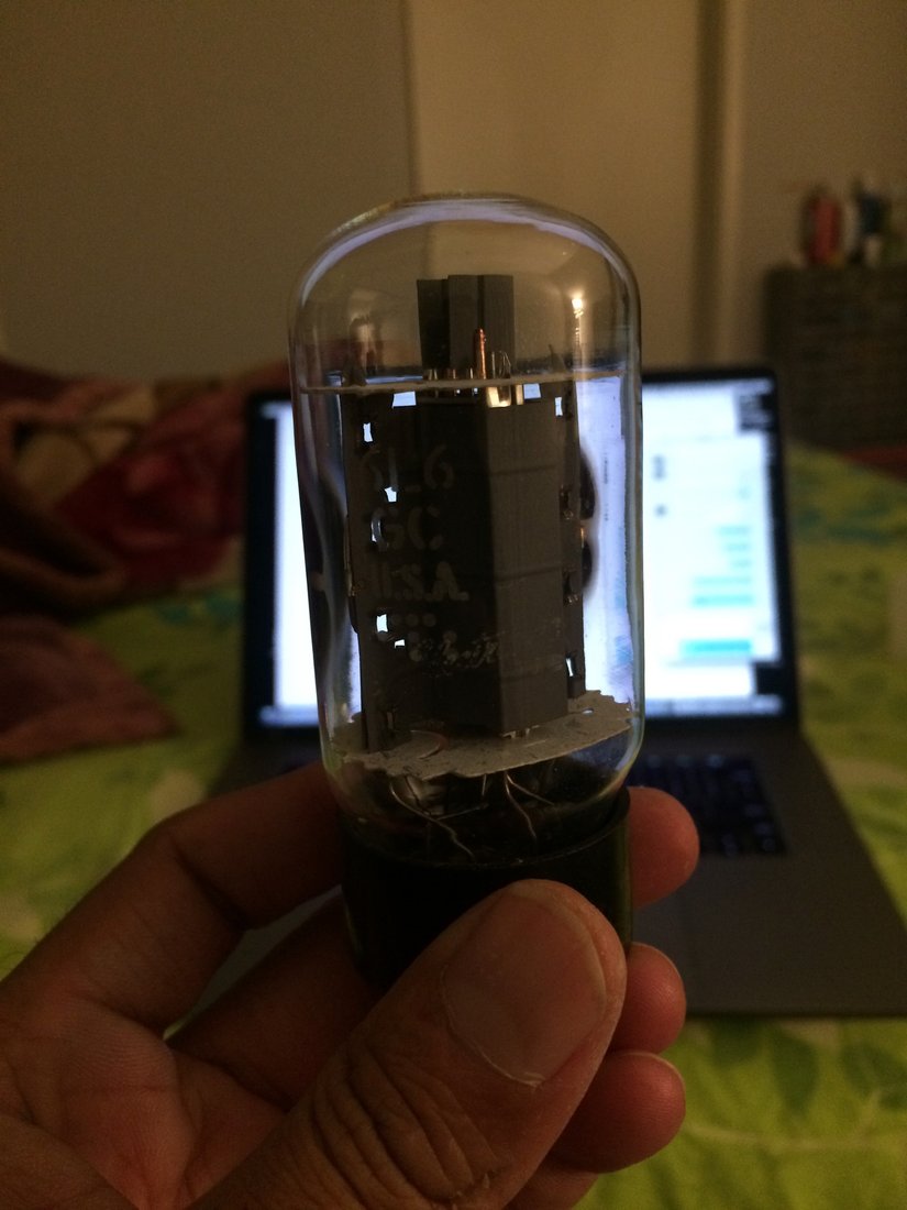
⚠ Danger — plate dissipation and touch temperature. The pass tubes carry both high voltage and real current simultaneously by design — that is where a series regulator’s “wasted” power goes. Expect the tube envelopes and their sockets to run hot during normal use; do not touch them in-circuit, and let the unit cool before reaching near V2/V3 even after power-down. Vol 5 covers replacement/testing procedure for tired pass tubes (low emission or gassiness shows up as an inability to reach 400 V, or as sluggish/noisy regulation).
2.2.4 Table — the series-pass stage at a glance
Table 1 — Table — the series-pass stage at a glance
| Item | Value / designator | Notes |
|---|---|---|
| Device count | 2 | V2, V3 |
| Type | 6L6GC beam-power pentode | Heath part 411-8 |
| Connection | Pentode (not triode-strapped) | Lower dropout than triode connection |
| Configuration | Parallel (plates common, cathodes common) | Splits plate current/dissipation across two tubes |
| Plate supply | Raw B+ bus, ≈ 600 V DC no-load | From the voltage doubler, §6 |
| Screen supply | Independent half-wave supply, D1/D2 | §7 — kept separate from the plate circuit |
| Grid drive | From V1 (6AU6) plate, through suppressor resistors R4 (V2), R5 (V3) | §5 |
| Output node | Cathodes → B+ output post, via metering | M2 (0–150 mA) reads this current directly |
| Continuous rating | 100 mA (125 mA intermittent), combined | No active current limit — §12 |
2.3 The Control (Error) Amplifier — the 6AU6
2.3.1 A DC-coupled comparator, not an audio amplifier
V1, a single 6AU6 pentode, is the SP-2717A’s entire error-amplifier stage — one tube doing the job that in a modern design would be an op-amp. It is a DC voltage-feedback amplifier: not “amplifier” in the audio sense of passing a signal, but in the control-theory sense of turning a small DC error voltage (how far the sampled output has drifted from the reference) into a large corrective swing at its plate, which then drives the pass-tube grids.
The 6AU6’s control grid receives a sample of the B+ output taken from the B+ VOLTS control, R12 — a 500 kΩ front-panel potentiometer that does double duty: it sets how much of the output voltage is compared against the reference (which is how the front-panel B+ VOLTS knob actually sets the output voltage — turning R12 changes the comparison ratio, not the raw supply), and its divider network is referenced not to chassis ground but to the regulated −300 V rail off the zener stack. Feeding a negative reference into the bottom of the divider, rather than grounding it, is what lets a modest value of tube-grid bias produce a comparison across the full 0–400 V span without requiring absurdly large divider resistances.
The 6AU6’s plate output drives the two 6L6GC control grids in parallel, through the individual suppressor resistors R4 and R5 mentioned above. Those suppressors exist to prevent parasitic VHF oscillation between the paralleled pass tubes — a classic failure mode any time two power tubes share a grid drive node — not to shape the DC control signal itself.
2.3.2 Screen feedforward — chasing near-zero output impedance
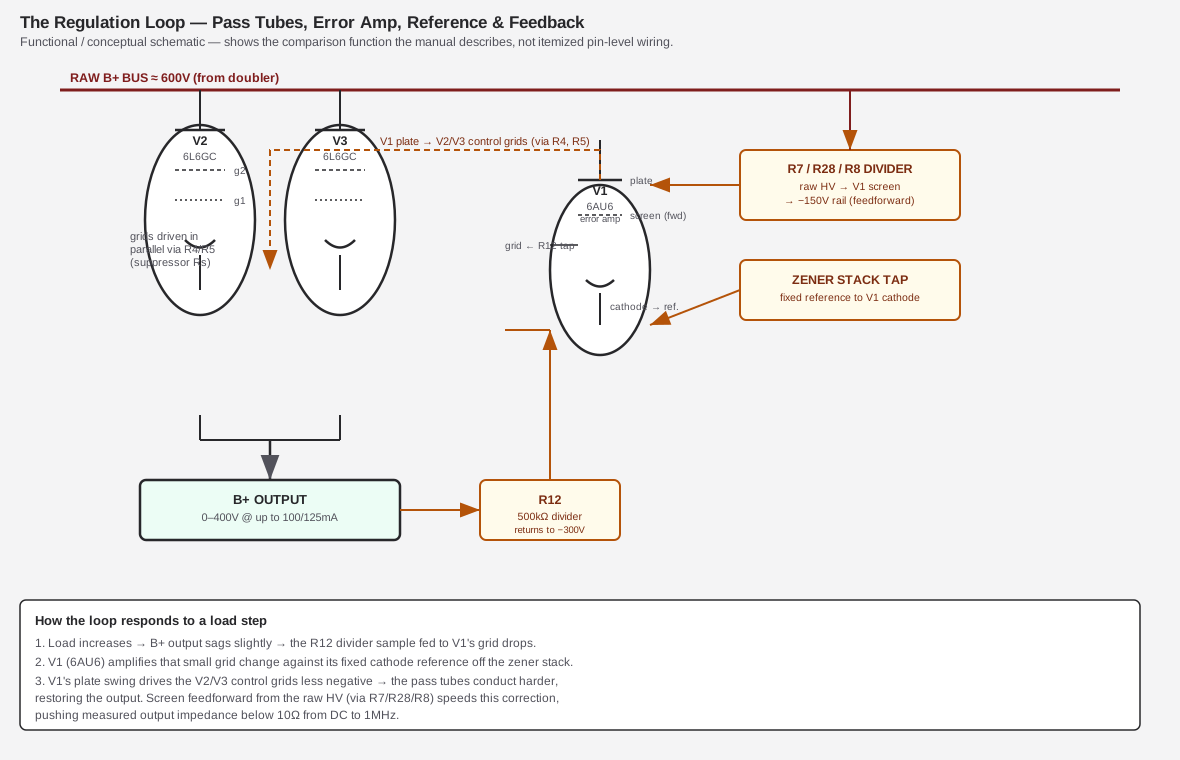
The one refinement in this stage worth calling out on its own is the 6AU6’s screen-grid feed. Rather than tying V1’s screen to a fixed, well-filtered reference (the “textbook” way to keep a pentode’s characteristics stable), the manual routes it through a divider — resistors R7, R28, and R8 — connected between the raw, unregulated HV source and the regulated −150 V rail. In other words, V1’s screen voltage rides up and down with the raw supply’s own sag under load, rather than staying fixed.
This is a deliberate feedforward technique layered on top of the primary feedback loop. Pure negative feedback alone always has finite loop gain, and finite loop gain means the output can never be perfectly independent of load or line disturbances — there is always some residual error, however small, that the loop needs in order to generate the correction. By additionally injecting a sample of the raw supply’s own variation directly into the error amplifier’s screen circuit, the design partially cancels disturbances before they even show up as an output error for the feedback loop to chase. The manual’s own spec sheet is the proof this works: output impedance under 10 Ω from DC to 1 MHz, and load regulation under 1% across the entire 100–400 V span from no load to full load — figures that are difficult to reach from feedback alone in a single-stage tube error amplifier. Vol 1 quotes the full “Representative Output Impedance Curves” spec; this section is where that number actually comes from.
The manual describes this comparison function — output sample vs. reference, driving the pass-tube grids — without spelling out every intervening node. The schematic above shows the functional topology (grid from the R12 divider, cathode from a fixed zener-stack tap, screen fed forward from the raw HV via R7/R28/R8); treat it as conceptual rather than a pin-exact trace of the original PCB.
2.3.3 Table — the control amplifier at a glance
Table 2 — Table — the control amplifier at a glance
| Item | Value / designator | Notes |
|---|---|---|
| Device | 1 × 6AU6 pentode | Designated V1 |
| Function | DC error/comparison amplifier | Not an AC signal amplifier |
| Grid input | Sample of B+ output via R12 (500 kΩ, B+ VOLTS control) | Divider returns to regulated −300 V |
| Reference | Zener stack (ZD1–ZD10), §4 | Replaces the IP-32’s 0A2 VR tubes |
| Screen supply | R7 / R28 / R8 divider, raw HV → −150 V rail | Feedforward — chases zero output impedance |
| Plate output | Drives V2/V3 control grids in parallel | Through suppressor resistors R4, R5 |
| Resulting spec | Output impedance < 10 Ω, DC–1 MHz; load reg. < 1%; line reg. < ±1% | Manual Specifications page |
2.4 The Voltage Reference — Ten Zener Diodes in Series
2.4.1 From gas tubes to silicon: retiring the 0A2
Every regulator needs something to compare against — a reference that is itself stable enough that the loop’s accuracy is limited by the reference, not by the amplifier. In the IP-32 generation, that reference was two 0A2 cold-cathode gas voltage-regulator tubes, glass envelopes filled with a gas mixture that strikes a stable glow discharge and holds a fixed voltage drop across a wide current range — the tube-era equivalent of a zener diode, and a fixture of regulated tube power supplies for decades.
By 1982, that job had migrated entirely to silicon. The SP-2717A’s reference is a series stack of ten zener diodes, ZD1 through ZD10 (Heath part 56-47, type MZ-1000-23 or equivalent), fed from the same silicon negative supply (§8) that also produces the negative/bias rail. There is no glow discharge, no gas fill, no tube warm-up delay in the reference path — just a string of silicon junctions held in avalanche breakdown by the current through them.
2.4.2 Building −150 V and −300 V from one string
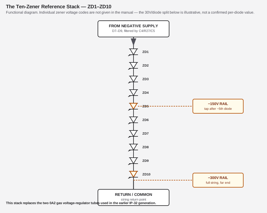
The ten-diode stack develops two regulated rails simultaneously: −150 V and −300 V, both used elsewhere in the circuit (the −300 V rail anchors the B+ VOLTS divider’s return point and the bleeder, §11; the −150 V rail feeds the screen-feedforward divider, §3). Running one long series string and tapping it at an intermediate point, rather than building two entirely separate zener regulators, is an economical way to get two related, well-regulated negative rails from a single current path.
The manual’s parts list gives the zener part number and quantity but does not itemize the individual breakdown voltage of each of the ten diodes. If the stack divides its total drop evenly, each diode would be dropping on the order of 30 V (300 V ÷ 10), with the −150 V tap coming off roughly the fifth diode in the string — that is a reasonable engineering inference from the two published rail voltages and the diode count, not a confirmed per-diode figure. Treat any specific per-zener voltage as illustrative rather than verified.
2.4.3 Why a stack of small zeners instead of one big one
Stacking modest zener diodes in series to reach a few hundred volts of total regulated drop, rather than sourcing one exotic high-voltage zener, is a common and sensible design choice: ordinary, inexpensive, widely available zener parts in the tens-of-volts class stack cleanly, and the failure mode of a shorted zener in a long series string is more forgiving (the remaining diodes still hold most of the intended voltage) than the failure of a single monolithic high-voltage part. It is also, per the restoration record, the SP-2717A’s most commonly documented failure point: zeners running hot against the printed circuit board have been known to fail shorted, shifting both reference rails and degrading regulation across the board. Vol 5 covers the documented fix — standing the zener bodies off the PCB surface for better cooling — in the context of a full recap-and-refurbish pass.
⚠ Danger — a shifted reference is a shifted output, at full voltage. A shorted or drifted zener anywhere in this stack changes the −150 V and/or −300 V rails the entire regulation loop is built on. Depending on which diode fails and how, the practical symptom ranges from a B+ output that will not reach the dialed setpoint to one that cannot be pulled down at all — and in either case the circuit is still carrying full raw B+ while you diagnose it. Power down, discharge, and verify before probing this board.
2.4.4 Table — the reference stack at a glance
Table 3 — Table — the reference stack at a glance
| Item | Value / designator | Notes |
|---|---|---|
| Device count | 10, in series | ZD1–ZD10 |
| Type | Zener diode, MZ-1000-23 or equivalent | Heath part 56-47 |
| Fed from | Negative supply (D7–D9, filtered C4/R27/C5), §8 | All-silicon |
| Rails produced | −150 V (intermediate tap) and −300 V (full string) | Both regulated |
| Replaces | Two 0A2 gas voltage-regulator tubes (IP-32 generation) | The defining generational change, per Vol 6 |
| Documented failure | Shorted zener(s), attributed to running hot against the PCB | Fix: stand off the board for cooling — Vol 5 |
2.5 Closing the Loop
2.5.1 Signal-path walkthrough: a load step from no load to 100 mA
Trace the loop through one concrete disturbance — the B+ output going from no external load to a full 100 mA draw, with the B+ VOLTS control left untouched:
- The load increases. Current through the pass tubes’ cathode circuit rises; absent any correction, the additional voltage dropped across the tubes’ own internal resistance (plus any series impedance in the output path) would pull the B+ output down slightly.
- The R12 divider sees it first. Because R12 continuously samples a fixed fraction of the B+ output, any sag at the output shows up immediately, scaled down, at V1’s control grid.
- V1 (the 6AU6) amplifies the error. With its cathode held at a fixed reference tap off the zener stack, a small negative-going shift at the grid produces a larger positive-going swing at V1’s plate (standard pentode inverting-amplifier behavior).
- That swing drives the pass-tube grids less negative. V2 and V3 conduct harder, dropping less voltage across themselves for the same current — which is exactly the correction needed to push the output back up toward the setpoint.
- The screen-feedforward path (§3) helps in parallel. Because V1’s screen is also riding on a sample of the raw HV bus, any simultaneous sag in the raw supply itself (which also happens under heavier load, since the doubler’s own regulation is imperfect) is partially cancelled before it ever becomes a feedback error for step 2–4 to chase.
- Steady state re-establishes. The loop settles with the output back within the manual’s quoted load-regulation figure — under 1% change from no-load to full-load, anywhere in the 100–400 V range — and the new, slightly different grid bias on V2/V3 holding that higher conduction level.
The same chain runs in reverse for a load decrease, and an analogous chain (line regulation, quoted at under ±1% for a ±10% mains change) runs when the AC input itself moves rather than the load.
2.5.2 What “output impedance” means here
The manual expresses the loop’s dynamic performance not just as a single load-regulation percentage but as output impedance versus frequency — under 10 Ω from DC to 1 MHz — because a real load is rarely a clean DC step; it can be a transient, a ripple component, or an AC signal riding on the DC rail (exactly the kind of thing a tube circuit under test on this bench might present). An output impedance figure captures how stiff the supply looks across that whole frequency range, not just at DC. Keeping that figure low across such a wide bandwidth — well beyond audio, into the low end of RF — is precisely what the screen-feedforward trick in §3 is there to buy: pure feedback loses gain (and therefore stiffness) as frequency rises, while a feedforward path that samples the raw supply directly does not have that rolloff problem, so combining the two extends low output impedance further up in frequency than feedback alone would manage.
2.6 The Raw B+ Supply — a Silicon Voltage Doubler
2.6.1 Topology
The B+ output post is not fed directly from a rectified-and-filtered transformer secondary; it is fed from the regulated side of the loop described above, whose unregulated input is a full-wave silicon voltage doubler: diodes D3, D4, D5, D6 and reservoir capacitors C2 and C3 (68 µF each). This doubler is entirely silicon — a deliberate departure from the IP-32 generation, which used a mix of silicon diodes and two selenium rectifiers for the equivalent stage. There is no selenium anywhere in the SP-2717A.
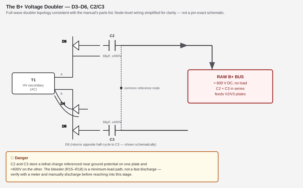
A voltage doubler is the natural choice here because it lets Heath use a comparatively modest HV transformer winding and still reach the roughly 600 V raw bus the pass tubes need in order to have headroom to regulate a full 400 V output — a straight full-wave rectifier off the same winding would deliver only about half that raw voltage. The tradeoff, inherent to any doubler, is that the two reservoir capacitors each see substantial ripple current and the full raw voltage is only present across the series combination of C2 and C3 — each individual capacitor sees a smaller fraction of the total, but still enough that both are HV-rated parts.
2.6.2 Ripple, reservoir sizing, and the ≥450 V rule
The manual documents the doubler’s raw output as approximately 600 V at no load, feeding the 6L6GC plates. Sixty-eight microfarads is a substantial reservoir value for an HV electrolytic of this era, chosen to keep ripple on the raw bus low enough that the regulation loop (§5) does not have to work overtime rejecting it, and to keep the pass tubes’ plate-to-cathode voltage from sagging visibly between AC half-cycles under full 100 mA load.
Because C2 and C3 sit directly across a raw bus that can reach roughly 600 V, any replacement part needs real HV headroom — the working consensus among restorers, corroborated by the doubler’s own raw-voltage figure, is 450 V-class parts as a floor, 500 V-class preferred. Vol 5 carries the full recap bill of materials (C1/C4/C5/C8/C10 alongside C2/C3) and the documented failure patterns for this generation of Heath electrolytics.
⚠ Danger — the doubler reservoir caps are the single most lethal node in this chassis. C2 and C3 sit at the raw ~600 V bus, upstream of every protective/regulating element described in this volume. They are large enough (68 µF each) to hold a dangerous charge for a long time after power-down. The bleeder chain (§11) discharges them only slowly, as a side effect of being a minimum-load path — it is emphatically not a fast-discharge safety circuit. Always verify zero volts with a meter, from both C2 and C3 to common, before working anywhere near this stage.
2.6.3 Table — the raw B+ supply at a glance
Table 4 — Table — the raw B+ supply at a glance
| Item | Value / designator | Notes |
|---|---|---|
| Topology | Full-wave silicon voltage doubler | D3, D4, D5, D6 |
| Reservoir C2 | 68 µF electrolytic | Heath part 25-956; ≥450 V-class replacement |
| Reservoir C3 | 68 µF electrolytic | Heath part 25-956; ≥450 V-class replacement |
| Raw output | ≈ 600 V DC, no load | Feeds V2/V3 plates directly |
| Rectifier material | All-silicon | No selenium in this generation (unlike the IP-32) |
| Downstream load | Series-pass tube plates | The pass tubes drop the difference to the regulated output |
2.7 The Screen-Grid Supply for the Pass Tubes
A dedicated, independent screen-grid supply for V2/V3 is what makes running them as true pentodes (§2) practical. Silicon diodes D1 and D2 rectify half-wave off the transformer, filtered by C1A / R1 / C1B, and fed through parasitic-suppressor resistors R2 and R3 to the two 6L6GC screen grids. Keeping this circuit separate from the raw B+ plate supply — rather than deriving screen voltage from the same doubler output through a dropping resistor — means the screens see a comparatively clean, independently filtered rail rather than one entangled with the plate circuit’s own load- dependent behavior, which matters for keeping the pass tubes’ characteristics predictable across the full range of plate current the regulator asks of them.
2.7.1 Table — the screen supply at a glance
Table 5 — Table — the screen supply at a glance
| Item | Value / designator | Notes |
|---|---|---|
| Rectification | Half-wave, silicon | D1, D2 |
| Filter | C1A / R1 / C1B | 22 µF class electrolytic (C1) — see Vol 5 recap list |
| Suppressor resistors | R2 (to V2 screen), R3 (to V3 screen) | Parasitic-oscillation suppression, same role as R4/R5 on the grids |
| Feeds | Screen grids (g2) of V2 and V3 | Independent of the plate/B+ circuit |
2.8 The Negative / Bias / Reference Supply
2.8.1 The chain
Silicon diodes D7, D8, D9 rectify a negative-going DC rail, filtered by C4 (22 µF), R27, and C5 (47 µF). This negative rail is the raw material for two entirely separate downstream jobs:
- It feeds the zener reference stack (§4), which regulates it down into the −150 V and −300 V rails the control amplifier and dividers rely on.
- It also supplies the front-panel C− (bias) output — 0 to −100 V DC at 1 mA — through the C− VOLTS control, R19 (50 kΩ).
2.8.2 The bias output’s own current limit
Unlike the B+ output (§12 explains why B+ has none), the C− output is current-limited: it feeds through a dedicated 22 kΩ resistor, R20, whose explicit purpose per the manual is to “prevent damage in case the negative output circuit should be overloaded or accidentally shorted.” That distinction — B+ unprotected beyond a fuse, C− actively current-limited by a series resistor — is worth internalizing now; it comes up again in §12’s protection-philosophy discussion and in Vol 4’s operating procedure.
The part actually at risk from bias-output abuse is not R20 (which is doing its job by limiting current) but the front-panel C− VOLTS pot, R19 — restorers report it can be burned out by loading the negative output beyond its 1 mA rating, since a wirewound or carbon pot dissipating fault current at the low end of its travel has comparatively little thermal mass to absorb it.
2.8.3 Table — the negative/bias supply at a glance
Table 6 — Table — the negative/bias supply at a glance
| Item | Value / designator | Notes |
|---|---|---|
| Rectification | Silicon, D7, D8, D9 | Negative-going |
| Filter | C4 (22 µF) → R27 → C5 (47 µF) | |
| Feeds | Zener reference stack (§4) AND C− front-panel output | Shared negative rail |
| C− output range | 0 to −100 V DC @ 1 mA | Special-taper C− VOLTS control for fine low-bias adjustment |
| C− current limit | R20, 22 kΩ | Explicit short-circuit protection — B+ has no equivalent |
| Vulnerable part under abuse | R19 (50 kΩ C− VOLTS pot) | Documented restorer failure mode from loading the bias output |
2.9 Startup Behavior — Standby, Filament Warm-Up, and the Loop
2.9.1 Two switches, two transformers, one purpose
The front panel carries two power-related switches: AC POWER (S1) and DC ON–STANDBY (S2). Their relationship to the two power transformers is the whole point of having two switches instead of one. T1 (the HV/screen transformer) and T2 (the filament transformer) are physically separate windings on separate iron, and the manual’s own Introduction explains why: separate transformers let the filament stay on with the DC (B+) switched to STANDBY, avoiding repeated tube warm-up. Read together with the front-panel control layout, the practical behavior is: AC POWER brings the whole instrument to life, filaments included, while DC ON–STANDBY specifically gates whether the high-voltage side — the doubler, and therefore the pass-tube plates — is actually engaged. STANDBY leaves V1, V2, and V3 sitting warm, cathodes at full emission temperature, with no B+ on their plates; DC ON connects the raw bus and lets the regulation loop actually start working.
2.9.2 Why this matters for the loop, not just for tube life
The tube-life argument is the one the manual states explicitly, and it is real: repeatedly cycling a tube’s heater from cold every time the instrument is powered up subjects the cathode coating to thermal stress it would not see if the heater simply stayed warm across a bench session while only the HV toggles. But there is a second, quieter benefit that falls directly out of this volume’s subject — the regulation loop itself behaves better when it never has to work through a cold start.
A vacuum tube’s characteristics — plate resistance, transconductance, achievable emission current — are all functions of cathode temperature, and cathode temperature does not snap to its operating value the instant a heater is powered; it ramps over on the order of tens of seconds. If B+ were applied to the 6L6GC pass tubes and the 6AU6 error amplifier while their cathodes were still cold and their characteristics still drifting, the regulation loop would be trying to hold a stable output using control elements whose own gain and conduction were themselves unstable — a genuine recipe for overshoot, undershoot, or transient instability during the first seconds after power-up. By keeping the filaments continuously warm (AC POWER on, DC held at STANDBY) and only then switching DC ON once the tubes have reached full emission, the SP-2717A always brings its loop up against tubes that are already at their normal operating point. The loop’s first moment of closed-loop control is also its first moment of predictable control.
This is not incidental to how the instrument is meant to be used: the manual’s own recalibration procedure (Vol 5 covers it in full) explicitly instructs the technician to warm up the filaments for several minutes before switching DC ON, precisely because the ZERO VOLTAGE ADJUST and 400 VOLT ADJUST calibration pots are being set against the loop’s settled behavior, not its warm-up transient.
2.10 Reading the Loop from the Front Panel
Everything this volume has described so far lives inside the chassis, but the two panel meters give a direct, real-time window into it. M1, the voltmeter (part 407-123), is a dual-scale 0–400 V / 0–150 V DC meter accurate to ±3% of full scale; the front-panel VOLTMETER switch, S3, decides whether it is reading the B+ output or the C− (bias) output, with a colored indicator lamp — red for B+, amber for C− — driven off the filament transformer T2 so the operator always knows at a glance which rail M1 is currently showing. M2, the milliammeter (part 407-124), reads 0–150 mA at ±2% of full scale and is wired directly into the B+ cathode return — meaning it is not measuring some derived or scaled quantity, it is reading the actual current flowing through the V2/V3 cathode circuit described throughout §2–§5, in real time.
That placement makes M2 more than a convenience readout. Because §12 establishes that the B+ output has no active current limit — nothing standing between an overload and the pass tubes except the mains fuse and the tubes’ own dissipation ceiling — M2 is, in a very literal sense, the operator’s only real-time instrumentation for how hard V2 and V3 are working at any given moment. On a modern bench supply with automatic current fold-back, the current meter is informational; on the SP-2717A, watching M2 while dialing in an unfamiliar or reactive load is closer to a safety practice than a convenience — it is the only feedback path that exists between the pass tubes’ actual dissipation and a human being who can turn the B+ VOLTS knob back down.
2.11 The Bleeder — Minimum Load for Control
2.11.1 Why a regulator needs a minimum load at all
A series-pass regulator built around vacuum tubes has a subtlety that a solid-state design does not share as sharply: the pass tubes need to be conducting some minimum current in order for the control loop to have any authority over them. At true zero external load, with nothing drawing current from the B+ output post, there is a risk that the pass tubes’ conduction drops so low that the error amplifier loses meaningful control range — the loop can ask for less current, but there is essentially nothing left to reduce.
The SP-2717A solves this with a four-resistor bleeder chain, R15 through R18, each 27 kΩ, 2 W, wired in series (≈108 kΩ total) between the raw B+ bus and the regulated −300 V rail. This provides a small, constant, resistive current path that keeps the pass tubes lightly loaded even with zero external draw, which is enough to keep the regulation loop in control across the full 0–400 V range regardless of what — if anything — is connected to the front-panel output posts.
This is the same four-resistor, 27 kΩ/2 W bleeder used in the earlier IP-32 generation, unchanged across the family; there is no primary-source evidence that this value ever shifted across manual revisions, despite one unverified claim to that effect circulating about “the current-limit circuit and bleeder resistor” differing between printings. Treat any such claim as unsupported until a specific dated schematic revision proves otherwise.
⚠ Danger — the bleeder is not a safety discharge circuit. R15–R18 draw only a few milliamps continuously — enough to keep the regulator biased into control, nowhere near enough to rapidly discharge C2/C3 after power-down. Depending on component tolerances and exact loading, meaningful voltage can persist on the raw bus for a surprisingly long time. Always verify zero volts with a meter before reaching into this chassis; never assume the bleeder has done the job for you.
2.11.2 Table — the bleeder at a glance
Table 7 — Table — the bleeder at a glance
| Item | Value / designator | Notes |
|---|---|---|
| Resistors | R15, R16, R17, R18 | Each 27 kΩ, 2 W |
| Configuration | Series string | ≈108 kΩ total |
| Connected between | Raw B+ bus and regulated −300 V rail | Not raw B+ to common |
| Purpose | Minimum-current path to keep V2/V3 in the loop’s control range at no external load | Not a discharge safety circuit |
| Stability across the family | Identical value in the IP-32 generation | No verified evidence of a changed bleeder value across printings |
2.12 Protection Philosophy — Why There Is No Active B+ Current Limit
2.12.1 B+ vs. C−: two very different protection strategies
It is easy to assume a regulated supply this sophisticated has active, fold-back-style current limiting on every output — many modern bench supplies do. The SP-2717A does not, and the asymmetry between its two DC outputs is worth stating precisely:
- The C− (bias) output is current-limited by design — the 22 kΩ series resistor R20, explicitly documented as short-circuit protection (§8).
- The B+ output has no dedicated active current-limit or fold-back circuit at all. Protection is limited to the mains fuse (1.5 A slow-blow at 110–130 V AC; 1.0 A recommended at 220–260 V AC) and the inherent plate-dissipation ceiling of the 6L6GC pass tubes themselves — which is precisely why the B+ rating is expressed as 100 mA continuous, 125 mA intermittent, rather than as a hard current limit the circuit actively enforces.
2.12.2 Why this is a reasonable design, not an oversight
A dedicated active current-limit circuit for a several-hundred-milliamp, several-hundred-volt B+ rail adds real complexity — sense resistors in a high-voltage path, an additional control stage, more failure modes of its own — for a benefit that, in 1982, a simple slow-blow fuse plus generous pass-tube dissipation margin already delivered adequately for the instrument’s intended use: bench breadboarding of tube circuits, not industrial duty cycling at the ragged edge of the rating. The tradeoff is that the operator is the current limit on B+: exceeding 100 mA continuous (or briefly 125 mA) is a matter of tube heating and, eventually, tube or fuse failure, not a graceful, self-protecting current fold-back the way a modern bench supply would behave.
⚠ Danger — B+ overload is a slow failure, not an instant shutdown. Because there is no active current limit, drawing sustained B+ current above the rated 100 mA does not trip a protective circuit — it simply runs the pass tubes hotter than their design margin, which can shorten tube life or, in an extreme or prolonged overload, damage the tubes or other B+-path components before the fuse ever sees enough current to open. Respect the 100 mA continuous / 125 mA intermittent rating as a real limit, not a suggestion, and watch M2 (the B+ milliammeter) when driving an unfamiliar or reactive load. Vol 4 covers safe operating margins in more detail.
2.12.3 Worked example: where the watts go
The shape of the B+ rating — a current ceiling backed only by tube dissipation, not an active limit — becomes concrete with a little arithmetic. The pass tubes (§2) drop the difference between the raw ~600 V bus and whatever voltage the front panel is dialed to, and that dropped voltage, multiplied by the current flowing, is exactly the power the two 6L6GCs together must dissipate as heat. Using the manual’s own raw-bus figure (≈600 V DC, no load) and the rated B+ current ceiling, a few representative operating points:
Table 8 — operating points
| B+ VOLTS setting | Raw bus (no-load figure) | Voltage dropped across V2/V3 | B+ current | Total pass-tube dissipation | Per-tube (2 in parallel) |
|---|---|---|---|---|---|
| 400 V | ≈600 V | ≈200 V | 100 mA | ≈20 W | ≈10 W |
| 200 V | ≈600 V | ≈400 V | 100 mA | ≈40 W | ≈20 W |
| 50 V | ≈600 V | ≈550 V | 100 mA | ≈55 W | ≈27.5 W |
| ~0 V (fault / near-short at the output post) | ≈600 V | ≈600 V | up to 125 mA (intermittent rating) | up to ≈75 W | up to ≈37.5 W |
This table is arithmetic derived from the manual’s own raw-bus and current figures — it is not a power table the manual publishes. The ≈600 V raw-bus figure is quoted for no load; under real load the doubler’s own unregulated output sags somewhat (§6), so these numbers are illustrative upper-bound estimates, not measured values.
The pattern is the one every series-pass regulator has to respect: dissipation in the pass element is worst at the lowest output voltage and the highest current — exactly the condition a short, or a badly mismatched low-impedance load, on the front-panel B+ posts would create. General tube references commonly quote the 6L6GC’s plate dissipation rating in the neighborhood of 30 W per tube, which puts the near-zero-volts / full-current corner of the table above uncomfortably close to, or past, that figure for a sustained fault. Per this section’s core point, there is no circuit standing between that fault condition and the tubes — only the mains fuse and however long the tubes themselves can absorb the overage. That is the concrete, worked-arithmetic version of why the front-panel milliammeter (see “Reading the Loop from the Front Panel,” above) is not just a convenience on this instrument.
2.12.4 Table — B+ vs. C− protection compared
Table 9 — Table — B+ vs. C− protection compared
| B+ output | C− (bias) output | |
|---|---|---|
| Rating | 0–400 V DC @ 100 mA cont. / 125 mA int. | 0 to −100 V DC @ 1 mA |
| Active current limit? | No | Yes — series R20, 22 kΩ |
| What actually protects it | Mains fuse (1.5 A slow-blow @ 110–130 V; 1.0 A @ 220–260 V) + pass-tube dissipation ceiling | Dedicated current-limiting/short-protection resistor |
| Documented vulnerable component under abuse | Pass tubes V2/V3 (overheating), fuse (eventually) | C− VOLTS pot, R19 |
| Practical implication | Operator must respect the mA rating — there’s no automatic fold-back | Circuit is inherently forgiving of a momentary short |
2.13 The Loop, End to End — a Consolidated Reference Table
Every designator introduced in this volume, in one place, for quick lookup while probing the chassis or cross-checking against the schematic:
Table 10 — or cross-checking against the schematic
| Designator(s) | Device / value | Role in the regulation loop |
|---|---|---|
| V1 | 6AU6 pentode | Control (error) amplifier — compares B+ sample to reference |
| V2, V3 | 6L6GC beam-power pentode (×2) | Series-pass elements — the “variable resistor” |
| ZD1–ZD10 | Zener diode stack (×10) | Voltage reference — develops −150 V and −300 V |
| D1, D2 | Silicon diode | Screen-grid half-wave supply for V2/V3 |
| D3, D4, D5, D6 | Silicon diode | B+ voltage doubler |
| D7, D8, D9 | Silicon diode | Negative/bias/reference supply |
| C1A, C1B | Electrolytic, 22 µF class | Screen-supply filter |
| C2, C3 | Electrolytic, 68 µF each | Doubler reservoir — raw ≈600 V bus |
| C4 | Electrolytic, 22 µF | Negative-supply filter |
| C5 | Electrolytic, 47 µF | Negative-supply filter |
| R2, R3 | Resistor | Screen-grid parasitic suppressors |
| R4, R5 | Resistor | Control-grid parasitic suppressors |
| R7, R28, R8 | Resistor divider | Screen feedforward, raw HV → −150 V rail |
| R12 | 500 kΩ potentiometer | B+ VOLTS front-panel control / output-sample divider |
| R15–R18 | 27 kΩ / 2 W each (×4) | Bleeder — minimum load, raw B+ to −300 V |
| R19 | 50 kΩ potentiometer, special taper | C− VOLTS front-panel control |
| R20 | 22 kΩ | C− current-limit/short protection |
| R27 | Resistor | Negative-supply filter network |
Vol 3 places every one of these designators on the actual chassis/board layout and metering path; Vol 5 covers their documented failure modes and calibration touchpoints (R10 ZERO VOLTAGE ADJUST and R14 400 VOLT ADJUST, both downstream of this loop, set the divider ranges the R12 comparison operates within); Vol 4 covers safe day-to-day operation of the instrument this loop lives inside; Vol 6 carries the full generational comparison against the IP-32’s tube-VR version of the same loop.
Sources
- Heath Company, Model SP-2717A Regulated High Voltage Power Supply, operation/service manual 595-2705-02, © 1982 (Benton Harbor, Michigan) — Specifications, Circuit Description, and Parts List sections. Full text via Internet Archive: https://archive.org/details/Heathkit_SP-2717A_Regulated_HV_Power_Supply
- IP-2717A schematic (scanned), Nostalgic Kits Central: https://www.nostalgickitscentral.com/heath/schematics/heathkit_schema_ip2717a.pdf
- Bob Eckweiler (AF6C), “Heathkit of the Month #67 — IP-32 Bench HV Power Supply,” Orange County Amateur Radio Club, © 2015 — family lineage and IP-32 circuit detail used for the generational comparison: https://www.w6ze.org/Heathkit/Heathkit_067_IP32.pdf
- Radiomuseum, “Heath (Heathkit) Regulated HV Power Supply IP-2717A”: https://www.radiomuseum.org/r/heath_regulated_hv_power_supply_ip_2717a.html
- “Heathkit Zenith SP-2717A Power Supply Restore,” Lazy Electrons, 2018-06-02 — documented zener-stack and 6AU6 failure modes referenced in §4 and elsewhere: https://lazyelectrons.wordpress.com/2018/06/02/heathkit-zenith-sp-2717a-power-supply-restore/