Heathkit SP-2717A HVPS · Volume 3
Heathkit SP-2717A — Vol 3: Inside This Unit — Hardware, Devices, Outputs & Metering
Two 6L6GC beam-power pass tubes, a 6AU6 control amplifier, a stack of ten zener diodes standing in for a pair of long-gone VR tubes, and a chassis built to be turned on and left idling for hours without ever cooking a filament twice.
3.1 Scope of this volume
Vol 2 covered how the SP-2717A regulates — the feedback loop, the reference, the reasons a pentode beats a triode in a wide-range series regulator. This volume is the parts inventory: every active device on the chassis, both transformers, the exact numbers on every output post, both meters and the switch that shares one of them between two rails, every front-panel control, the mains input, and the fuse. Read it with a multimeter in one hand and the parts list in the other.
⚠ Danger — everything described here operates at up to ≈600 V raw DC on the doubler reservoir caps (C2, C3) and 400 V regulated at the B+ post. This is a hands-in-the-chassis volume for identification, not a live-troubleshooting guide — see Vol 4 §10 for the discharge-before-you-touch procedure and the shared
_shared/legal_ethics.mdHV discipline doc before opening the case with power applied.
Every fact in this volume traces to the manual’s Specifications, Tube And Diode Complement, and Parts List pages (part no. 595-2705-02, © 1982), cross-checked where noted against Bob Eckweiler’s Heathkit-of-the-Month #67 writeup on the IP-32 lineage. See Vol 6 for the full cheatsheet and the generational comparison against the IP-32.
Use this volume three ways: as a bench-ID checklist (§9 tells you what to look for to confirm you’re holding an SP-2717A/IP-2717A and not an older IP-32 or IP-17 without opening a manual at all), as a parts cross-reference (every designator that appears in Vol 2’s circuit theory and Vol 5’s refurb notes is defined here, once, with its physical location and Heath part number), and as an operating spec sheet (the numbers you need before you plug anything into the output posts — covered in full in Vol 4).
3.2 The active-device complement
The manual’s own heading for this table is “Tube And Diode Complement” — and that heading is the whole story of what generation this instrument belongs to. There is no voltage-regulator (VR) gas tube anywhere in this chassis, and there is no transistor anywhere in this chassis either. The SP-2717A is a hybrid: a vacuum-tube series-pass regulator riding on an all-solid-state rectifier and reference. That is the single fact that separates it from its 1962–67 ancestor, the IP-32 (Vol 6 has the full generational table).
3.2.1 Devices, by designator
Table 1 — Devices, by designator
| Designator | Device | Function | Heath part no. | Count |
|---|---|---|---|---|
| V1 | 6AU6 | Control (error) amplifier | — | 1 |
| V2, V3 | 6L6GC | Series-pass regulator tubes (pentode-connected) | 411-8 | 2 |
| D1, D2 | 1N2071 silicon diode | Screen-supply half-wave rectifier | 57-27 | 2 |
| D3–D6 | 1N2071 silicon diode | B+ voltage-doubler rectifier | 57-27 | 4 |
| D7–D9 | 1N2071 silicon diode | Negative/bias supply rectifier | 57-27 | 3 |
| ZD1–ZD10 | Zener diode (MZ-1000-23 or equiv.) | Series voltage-reference stack | 56-47 | 10 |
That is 2 tubes, 9 silicon rectifier diodes, and 10 zener diodes — 21 active devices total, none of them a transistor, none of them a gas-filled VR tube. Compare that to the IP-32’s complement of 2× 6L6 (paralleled, not the “GC” suffix), a 6BH6 control tube, 2× 0A2 VR tubes, 6 silicon + 2 selenium rectifiers, and a 6X4 tube bias rectifier — a visibly different, older recipe for the same job. Vol 2 covers why the pentode-connected 6L6GC was chosen over a triode connection for this role; this volume just inventories what’s there.
Note on tube designators — the manual’s own OCR is internally inconsistent in one spot (a Recalibration step mis-prints “V1 and V2 should glow” where it means the pass tubes), but the authoritative Tube And Diode Complement plus Parts List settle it unambiguously: V1 is the 6AU6 control amplifier; V2 and V3 are the 6L6GC pass tubes. Use that numbering — it’s what this whole series of volumes uses.
3.2.2 The two pass tubes — V2, V3 (6L6GC)
Two 6L6GC beam-power tubes sit between the raw high-voltage bus and the B+ output post, acting as a large variable resistance under control of V1. They are run as pentodes, with a dedicated screen-grid supply (below) — the manual is explicit that a pentode connection drops less voltage across the pass element than a triode connection would, which matters directly for how close to 0 V the regulator can still hold the loop in a wide-range 0–400 V design. See Vol 2 for the loop-gain reasoning; here, the hardware fact is simply: two 6L6GC, in the raw-HV-to-B+ path, dissipating real power as heat whenever the output is below the raw rail.
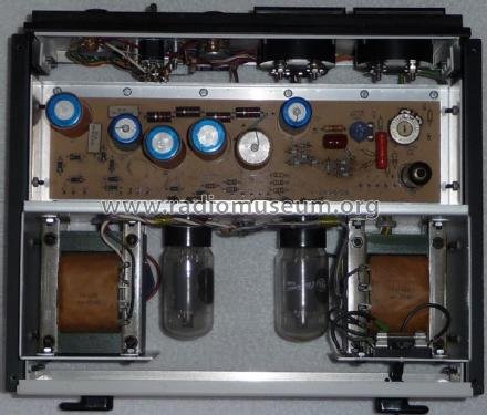
The “GC” suffix on 6L6GC is not decorative. It denotes a later, ruggedized version of the original 6L6 beam-power tube with a higher maximum plate-voltage rating and greater plate dissipation than a plain 6L6 — exactly the kind of headroom a wide-range, 0–400 V series regulator wants from its pass element, since the pass tube has to survive sitting at close to the full raw-rail voltage whenever the front panel is set for a low B+ output and the tube is dropping nearly all of it. That the IP-32 got by on plain paralleled 6L6 tubes in 1962 and the SP-2717A specified the GC variant in 1982 tracks the broader industry-wide shift toward the GC as the default 6L6 variant over that same twenty-year window — it’s not evidence of a different circuit topology, just a components upgrade riding on a part number that had become the standard by the 1980s.
⚠ Danger — the 6L6GC plates sit directly on the B+ rail. Even with the unit in STANDBY (filaments lit, DC switched off), the raw HV bus and the doubler caps can still hold a dangerous charge — see Vol 4 §10 before reaching into this area of the chassis.
A rough dissipation budget, worked from the manual’s own numbers. The manual states the doubler delivers roughly +600 V raw at no load. A series-pass regulator drops the difference between that raw rail and whatever the front panel is asking for across the pass tubes, as heat — so the tubes run hottest not at high B+ settings but at low B+ settings under load, where they’re absorbing nearly the full raw-to-output difference. Two illustrative points, using the raw-rail figure as a no-load approximation (the doubler caps will sag somewhat under real load, so treat this as a ballpark, not a lab-verified number):
- Near the top of the range — B+ set to 400 V, 100 mA load: the tubes drop roughly 600 − 400 = 200 V, so total pass-tube dissipation is on the order of 200 V × 100 mA ≈ 20 W combined, ~10 W per tube.
- Near the bottom of the specified load-regulation range — B+ set to 100 V (the low end the manual’s own load-regulation spec is stated over), still at 100 mA: the tubes drop roughly 600 − 100 = 500 V, so dissipation rises to on the order of 500 V × 100 mA ≈ 50 W combined, ~25 W per tube.
That’s a real spread, and it’s the underlying reason a well-used SP-2717A runs its pass tubes warm to hot in ordinary service — the closer you set B+ toward the low end of its range while pulling real current, the harder the tubes are working, not the easier. It also explains why the manual caps continuous current at 100 mA rather than something higher: dissipation, not rectifier or transformer capacity, is almost certainly the limiting design constraint on this pass stage. Vol 2 has the fuller regulation-loop treatment of where that dissipation comes from circuit-wise; this is just the hardware-level power budget.
3.2.3 The control amplifier — V1 (6AU6)
A single 6AU6 pentode is the DC error amplifier. It compares a sampled fraction of the B+ output — taken from the front-panel B+ VOLTS control (R12), a voltage divider referenced to the regulated –300 V rail — against the zener-stack reference, and drives the two 6L6GC control grids (through parasitic- suppressor resistors R4 and R5) to hold the output steady. Its own screen supply comes from an R7/R28/R8 divider straddling the raw +HV source and the regulated –150 V rail, chosen by the designers to make the loop’s own output impedance approach zero.
This is a documented failure point: a shorted 6AU6 is a known, restorer-confirmed fault that kills regulation entirely. If B+ won’t hold a setpoint, or drifts wildly, or won’t come up at all with the filaments warm and DC ON selected, check V1 before chasing anything else. See Vol 5 for the fuller failure-mode / refurb writeup.
3.2.4 The zener reference stack — ZD1–ZD10
Ten zener diodes, wired in series, sit across the negative supply and generate the regulated –150 V and –300 V reference rails that both the control amplifier and the front-panel divider networks work against. This stack is, functionally, a direct silicon-era replacement for the pair of 0A2 gas voltage-regulator tubes that did the identical job in the IP-32 twenty years earlier — same circuit position, same purpose, completely different technology. It’s the single clearest hardware tell that you’re looking at the ‘A’/SP generation and not the earlier IP-32/IP-17 generation.
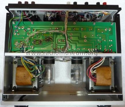
This stack is also a documented failure point, and for a specific, physical reason: restorers report zener diodes running hot enough against the PCB to fail shorted. The fix applied in at least one published restoration was simply to stand the zener bodies off the board for better cooling airflow rather than lying them flat against the copper. A shorted zener shifts the –150 V/–300 V reference rails and, downstream, the whole regulation setpoint — see Vol 5.
3.2.5 The rectifier diodes — D1–D9 (1N2071)
Nine 1N2071 silicon diodes (a roughly 600-PIV part, still a common substitute today) do three separate jobs in three separate sub-circuits, none of which share a physical rectifier stack:
- D1, D2 — half-wave, feed the pass-tube screen-grid supply.
- D3, D4, D5, D6 — full-wave voltage doubler, feed the raw B+ bus.
- D7, D8, D9 — feed the negative/bias/reference supply that the zener stack regulates.
None of the SP-2717A’s rectification is selenium and none of it is tube-based — a real change from the
IP-32, whose B+ rectifier used six silicon diodes alongside two selenium rectifiers.
Selenium rectifiers are a known hazardous-materials flag in vintage gear (off-gassing under fault
conditions); their complete absence here is one of the few unambiguous safety improvements the 1982
redesign delivered over the 1962 original. See the shared
_shared/legal_ethics.md doc for the hazardous-materials checklist
that still applies to the rest of the chassis (electrolytics, wiring insulation, line cord).
3.2.6 Block map — how the devices connect
                     T1 (power xfmr)
                          │
                          ▼
          D3–D6 doubler + C2/C3 (68 µF ea.)
                          │  raw ≈ +600 V (no load)
                          ▼
              V2, V3 — 6L6GC pass tubes ──────► B+ OUTPUT (0–400 V, 100/125 mA)
                          ▲
                          │ grid drive (R4, R5)
              V1 — 6AU6 control amplifier
                          ▲
             ┌────────────┴────────────┐
   B+ VOLTS (R12) sample      ZD1–ZD10 zener reference (–150 V / –300 V)
                                        ▲
                              D7–D9 + C4/C5 negative supply
                                        │
                          T2 (filament xfmr) ── filaments (V1, V2, V3)
                                        └──────► FILAMENT / AC OUTPUTS
                                        └──► C– VOLTS (R19) ──► C– (bias) OUTPUT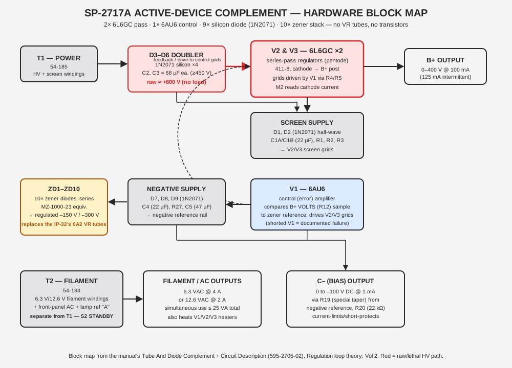
3.2.7 Where the parts physically live
The manual’s Circuit Description and Recalibration sections make the physical layout implicit even where they don’t diagram it directly. Three zones are worth keeping straight when you have the case open:
- The main circuit board carries the solid-state side of the design: the doubler diodes and their
reservoir caps, the screen-supply diodes and filter, the negative-supply diodes and filter, the full
zener reference stack, and the two internal calibration pots (R10, R14) — the manual is explicit that
those calibration pots are accessed “from the top of the circuit board.” This is also the board
photographed in
internals_pcb.jpgabove — the green-PCB solid-state cluster that is the single most reliable visual tell for this generation of the family. - The tube sockets (V1, V2, V3) and their associated parasitic-suppressor/grid resistors sit apart from the solid-state board, typically upright on the chassis deck where they can dissipate heat into open air rather than into a PCB — a layout consideration that matters directly for the zener-stack failure mode described above: those zeners already run hot from their own dissipation, and cook faster still if they’re thermally coupled to a board that also has three vacuum-tube heaters radiating nearby.
- The bleeder network (R15–R18) runs from the 6L6GC cathodes to the –300 V rail, physically bridging the tube deck and the solid-state board — see Vol 2 for why it’s there electrically (keeping the pass tubes in conduction at no load) and Vol 4 §10 for why it is not a substitute for manually discharging the doubler caps before you work in this area.
3.3 The two transformers — and why the filaments never have to cool
The SP-2717A carries two separate transformers, not one center-tapped unit doing double duty:
Table 2 — The SP-2717A carries two separate transformers, not one center-tapped unit doing double duty
| Designator | Heath part | Windings | Feeds |
|---|---|---|---|
| T1 | 54-185 | High-voltage + screen-grid | B+ doubler, screen supply |
| T2 | 54-184 | 6.3 V / 12.6 V filament, front-panel AC, lamp reference | Tube heaters, filament output posts, AC output posts, red/amber monitor-lamp drive (point “A”) |
Splitting the power supply into a dedicated HV transformer and a dedicated filament transformer is what makes the front-panel DC ON–STANDBY switch (S2) actually useful. STANDBY removes only the DC (high-voltage) side of the circuit — T2 and the filament string stay powered continuously as long as AC POWER (S1) is on. Practically: you flip to STANDBY between test setups or during a lunch break and the 6L6GC/6AU6 filaments stay warm, so you avoid the repeated cold-start thermal cycling that shortens tube life, and B+ comes right back up the instant you flip S2 back to DC ON — no multi-minute warm-up wait. This is stated explicitly in the manual’s Introduction as a deliberate design intent, not an incidental side effect of the parts on hand.
The IP-32 (Vol 6) shares this same two-transformer STANDBY architecture — a family trait shared with the IP-32, part of a lineage that traces back to the PS-4 (1957).
3.4 Outputs — exact numbers, exact posts
The SP-2717A has three distinct DC/AC output families, each brought to its own set of front-panel binding posts, and — critically — every output post is insulated from the chassis, so any of the three can be floated or referenced to a chosen “common” rather than to earth ground. That’s a deliberate design choice for breadboarding tube circuits where the B+ return, the bias return, and chassis ground are not always the same node.
3.4.1 B+ (high-voltage) output
Table 3 — B+ (high-voltage) output
| Parameter | Value |
|---|---|
| Voltage | 0 to 400 V DC, regulated |
| Current | 0 to 100 mA continuous; 125 mA intermittent |
| Load regulation | < 1% output variation, no-load to full-load, over 100–400 V DC |
| Line regulation | < ±1% for a ±10% change in the 120 V or 240 V AC source |
| Ripple / noise | < 10 mV RMS (ripple, jitter, and noise combined) |
| Output impedance | < 10 Ω, DC to 1 MHz |
What those numbers mean on the bench. A load-regulation spec of ”< 1% output variation, no-load to full-load” is a relative spec, so its absolute size scales with where B+ is set — at a 400 V setpoint it allows up to roughly 4 V of sag between no-load and a full 100 mA load; at a 100 V setpoint that same 1% is only about 1 V. Line regulation works the same way: ±1% for a ±10% swing in the AC mains means a typical brownout or a noisy shop circuit won’t move B+ by more than a few volts at most settings. The ripple/noise figure — under 10 mV RMS on a rail that can be sitting at 400 V — is a genuinely clean supply by tube-bench standards: at full scale that’s ripple roughly 40 dB below the DC level, well under what most tube audio or RF breadboard work needs to stay hum-free. The output-impedance spec (< 10 Ω from DC to 1 MHz) is the number that matters most if you’re driving a dynamic load — a Class AB output stage whose plate current swings with signal, for instance — because it tells you how much the B+ rail itself will sag and recover as that current swings, right up into the RF-adjacent frequency range.
⚠ Danger — there is no active current-limit or foldback circuit on the B+ output. The only protection is the mains fuse and the physical dissipation ceiling of the 6L6GC pass tubes — which is why the rating is capped at 100 mA continuous / 125 mA intermittent in the first place, rather than some larger number backed by an electronic limiter. Do not treat B+ as short-circuit-proof. A dead short on the B+ post is a fuse-blowing, tube-stressing event, not a graceful current-limited one.
3.4.2 C– (bias) output
Table 4 — C– (bias) output
| Parameter | Value |
|---|---|
| Voltage | 0 to –100 V DC, negative, adjustable |
| Current | 0 to 1 mA |
| Adjustment | C– VOLTS control, R19 (50 kΩ), special non-linear (“special taper”) taper for fine resolution at low bias values |
| Protection | Current-limited via R20 (22 kΩ) — the manual states this resistor “prevents damage in case the negative output circuit should be overloaded or accidentally shorted” |
The bias output is protected — unlike B+ — but the protection is one resistor, not a regulator loop, and the vulnerable component under abuse is the R19 pot itself, not R20. A commonly repeated restorer warning applies directly here: don’t load the bias output beyond its 1 mA rating, or you risk cooking R19.
3.4.3 Filament / AC output
Table 5 — Filament / AC output
| Parameter | Value |
|---|---|
| Option A | 6.3 V AC @ 4 A |
| Option B | 12.6 V AC @ 2 A |
| Combined | Both may be drawn simultaneously, provided total apparent power stays ≤ 25 VA |
Read the 25 VA ceiling carefully — it’s tighter than it first looks. Each individual rating, taken alone, is already right at that ceiling: 6.3 V × 4 A = 25.2 VA, and 12.6 V × 2 A = 25.2 VA. Both windings independently top out at essentially the same ~25 VA the combined spec allows. That means the “both may be drawn simultaneously” language is not offering you 4 A and 2 A at once (which would be roughly 50 VA, double the stated ceiling) — it’s saying you can split that one ~25 VA budget across both posts in whatever proportion a given circuit needs, not that each post independently gets its own full-rated allowance on top of the other. In practice: if a breadboarded circuit needs both a 6.3 V heater string and a 12.6 V string running at once, plan on drawing well under each post’s individual maximum from both simultaneously, not the full 4 A and 2 A together.
3.4.4 Output binding posts (full list)
Table 6 — Output binding posts (full list)
| Post | Purpose |
|---|---|
| Common | Return for B+ |
| + | B+ output |
| Common | Return for C– |
| – | C– (bias) output |
| 6.3 VAC | Filament, 4 A |
| 12.6 VAC | Filament, 2 A |
| Chassis Ground | Frame/earth reference — separate from the floating commons above |
All output posts are insulated from the chassis by design, so B+ and C– can be used as either a positive or negative source relative to whatever “common” node the breadboarded circuit needs — a deliberate feature for tube-circuit prototyping where the supply’s own ground reference shouldn’t force a topology on the circuit under test. Chassis Ground remains available separately for anything that genuinely needs an earth tie.
3.4.5 Floating outputs — what the insulated-post design buys you
Because B+ Common and C– Common are each independently insulated from chassis, the two DC outputs can be combined in more than one way on the bench, and it’s worth spelling out the patterns the design enables rather than leaving it as an abstract feature:
- Conventional grounded-cathode operation — tie B+ Common, C– Common, and Chassis Ground together at one point, and both outputs behave exactly like a normal lab supply referenced to earth. This is the default, lowest-risk configuration for most breadboard work.
- Grid-bias supply floated below a separate B+ common — leave B+ Common isolated from C– Common and tie C– Common instead to the cathode (or cathode-bias node) of the circuit under test, so the C– output delivers true fixed bias referenced to that node rather than to chassis. This is the textbook use case the “special taper” C– VOLTS pot (below) is tuned for.
- Stacked/series use for an extended total swing — because neither DC output has to return to chassis, a circuit that needs, say, a voltage referenced well below its own B+ return can use the C– output’s isolation to get there without a second supply, as long as the 1 mA bias current ceiling and the insulation ratings of the posts themselves aren’t exceeded.
⚠ Danger — floating an output away from chassis ground does not make it safer to touch — it can make it more dangerous, because a floated node’s true potential relative to earth (and relative to you, standing on the floor) is no longer obvious from the panel alone. Verify every floated node with a meter before touching it, every time, per Vol 4 §10.
3.5 Metering — one meter, two rails
The SP-2717A carries two panel meters, a design trait consistent across the whole family lineage.
3.5.1 M1 — the shared voltmeter
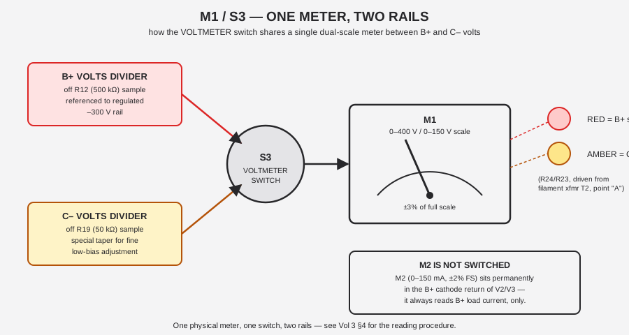
M1 (Heath part 407-123) is a dual-scale 0–400 V / 0–150 V DC voltmeter, accuracy ±3% of full scale. It is the only voltmeter on the panel, and it is time-shared between the two DC outputs by the front-panel VOLTMETER switch, S3: flip it one way and M1 reads B+ volts against its 0–400 V scale; flip it the other and M1 reads C– (bias) volts, presumably against the lower 0–150 V scale range for better resolution on the –100 V-max bias output. A colored indicator lamp tells you at a glance which rail you’re looking at without having to read the switch position — red = B+ is being monitored, amber = C– is being monitored. Both lamps are driven off resistors R24/R23, referenced to the filament transformer T2’s point “A.”
3.5.2 Why one shared voltmeter instead of two dedicated ones
It would have been simpler, circuit-wise, to give B+ and C– each their own dedicated meter — no switch, no lamps, no time-sharing. Heath didn’t do that here, and the choice is consistent with the rest of this family’s design economy: a single, reasonably-priced meter movement (407-123) does double duty across two ranges via a switch and a divider network, rather than paying for two meter movements to cover a job one can do time-shared. The tradeoff is exactly the one described above — you can’t watch B+ and C– at the same instant, only one or the other — which is a real limitation during, say, a calibration procedure that wants both readings in sequence (see Vol 5’s recalibration steps, which explicitly call out toggling S3 to B+ before each adjustment). M2, by contrast, does get its own dedicated movement, because current sense sits electrically in a completely different place in the circuit (the B+ cathode return) than either voltage-sense divider — sharing a meter there would have meant an entirely different, more complex switching arrangement for comparatively little benefit, since bias current at a 1 mA ceiling was apparently judged not worth metering directly at all.
3.5.3 M2 — the dedicated milliammeter
M2 (Heath part 407-124) is a 0–150 mA meter, accuracy ±2% of full scale, wired permanently into the B+ cathode return of the pass tubes. Unlike M1, M2 is not switched — it always and only reads B+ load current. There is no equivalent current meter for the bias output; at a 1 mA maximum rating, the bias current draw doesn’t get its own dedicated instrumentation.
3.5.4 Reading the panel in practice
Table 7 — Reading the panel in practice
| You want to know | Do this |
|---|---|
| B+ output voltage | S3 to B+ position → read M1 top (0–400 V) scale; red lamp confirms |
| B+ output current | Read M2 directly — always live, no switch needed |
| C– (bias) output voltage | S3 to C– position → read M1, presumably the 0–150 V scale for resolution; amber lamp confirms |
| C– output current | Not directly metered — respect the 1 mA rating by design margin, not by reading a meter |
⚠ Danger — M1’s 0–400 V scale is reading a rail that can genuinely be at 400 V DC relative to chassis-insulated commons. Treat the meter face as a live-voltage indicator, not a curiosity — if M1 is reading anywhere near full scale, the output posts it’s monitoring are at lethal potential.
3.5.5 What ±3%/±2% of full scale actually buys you
Meter accuracy specs are given as a percentage of full scale, not of the reading — which means the absolute uncertainty in volts or milliamps is constant across the whole scale, and gets proportionally worse the lower the actual reading sits below full scale. Worked out in absolute terms:
Table 8 — worse the lower the actual reading sits below full scale. Worked out in absolute terms
| Scale in use | Full scale | Accuracy spec | Absolute uncertainty (constant across the scale) |
|---|---|---|---|
| M1, B+ (0–400 V) | 400 V | ±3% FS | ±12 V, anywhere on the scale |
| M1, C– (0–150 V) | 150 V | ±3% FS | ±4.5 V, anywhere on the scale |
| M2 (0–150 mA) | 150 mA | ±2% FS | ±3 mA, anywhere on the scale |
This is exactly why the switch matters beyond convenience: reading the –100 V-max C– output on the 150 V scale, rather than trying to resolve it against the 400 V scale, keeps the meter’s fixed ±4.5 V absolute error down near 4.5% of a typical bias setting instead of the much worse fraction that same ±12 V error would represent against a small bias reading pulled off the coarser 400 V scale. Put another way: the dual-scale design isn’t just labeling convenience, it’s the manual’s own answer to the fact that a single-range meter accurate enough to read 400 V usefully is not accurate enough to read a 2–20 V bias setting usefully — hence a second, finer range sharing the same meter movement, switched in by S3. For anything genuinely precision-critical, though, treat M1 and M2 as bench-adequate, not metrology-grade, and cross-check against an external DMM — see Vol 5 for the recalibration procedure that assumes exactly that.
3.6 Front-panel controls
Table 9 — Front-panel controls
| Control | Designator | Type / value | Function |
|---|---|---|---|
| AC POWER | S1 | Toggle, part 60-24 | Mains power on/off — energizes T1 and T2 both |
| DC ON–STANDBY | S2 | Toggle, part 61-9 | Removes/restores the DC (HV) side only; filaments stay lit in STANDBY |
| VOLTMETER | S3 | Rotary switch | Selects whether M1 reads B+ or C– volts; drives red/amber lamps |
| B+ VOLTS | R12 | 500 kΩ potentiometer | Sets the B+ output setpoint, 0–400 V |
| C– VOLTS | R19 | 50 kΩ potentiometer, special (non-linear) taper | Sets the C– output setpoint, 0 to –100 V, with extra resolution near 0 V |
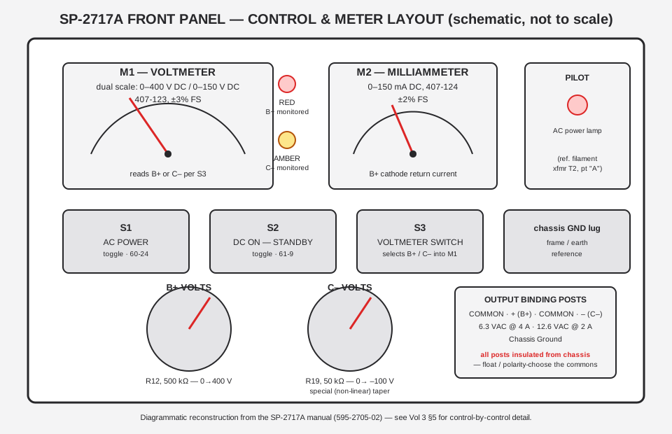
Two more controls live inside the chassis rather than on the panel — the calibration pots ZERO VOLTAGE ADJUST (R10) and 400 VOLT ADJUST (R14), both accessed from the top of the circuit board. Those belong to the calibration procedure, not day-to-day operation, and are covered in full in Vol 5.
3.6.1 Why the B+ and C– pots have such different values
The B+ VOLTS pot (R12) is 500 kΩ; the C– VOLTS pot (R19) is 50 kΩ — a 10:1 spread that lines up with the 10:1 spread between the two output ranges (0–400 V versus 0–100 V), which is unsurprising in a divider- based setpoint control. What’s more interesting is R19’s special non-linear (“special taper”) profile, called out explicitly by the manual rather than left as a generic linear pot. A linear taper spreads the control’s travel evenly across the full –100 V range, which is fine for coarse bias settings but leaves very little rotational travel — and therefore very little hand precision — available down in the low-single-digit-volt bias range where a lot of small-signal tube grid-bias work actually lives. A non-linear taper compresses the high end of the range and expands the low end, buying more usable knob rotation exactly where the operator needs the finest control. There is no equivalent non-linear callout for R12 — the B+ range doesn’t have the same “most of the interesting work happens near zero” shape that the bias range does.
3.7 Mains input & fuse
Table 10 — Mains input & fuse
| Parameter | Value |
|---|---|
| AC input | 110–130 V or 220–260 V, 50/60 Hz (wired-selectable; 240 V connection change documented in the manual) |
| Maximum power draw | 150 W |
| Fuse, 110–130 VAC operation | 1.5 A slow-blow (Heath part 421-25), located near transformer T2 |
| Fuse, 220–260 VAC operation | 1.0 A recommended |
The 110–130 V / 220–260 V range is wired-selectable, not switch-selectable — the manual documents an internal connection change to move the unit from one mains voltage family to the other, rather than a front-panel voltage-select switch. That matters for anyone acquiring a used unit with unknown history: there is no panel indicator telling you which way it’s currently strapped, so the only reliable way to know is to open the case and trace the transformer primary connections against the manual’s wiring diagram, or to measure carefully with the unit unpowered. Don’t assume a 120 V-market unit is still strapped for 120 V just because it’s in the United States — a well-traveled instrument, or one serviced by someone who didn’t relabel it, can be wired either way.
⚠ Danger — always verify which mains voltage the unit is wired for, and which fuse is installed, before applying power — especially on a unit with unknown or undocumented service history. A 1.5 A slow-blow fuse rated for 120 V operation gives materially less protection margin if the unit is actually strapped for 240 V, and vice versa.
3.7.1 Fuse sizing — does 1.5 A slow-blow make sense against 150 W?
Worth checking the arithmetic rather than just trusting the label. At 150 W maximum draw on a 120 V line, steady-state current is:
$$I = P / V = 150\ \text{W} / 120\ \text{V} \approx 1.25\ \text{A}$$
A 1.5 A fuse against a 1.25 A steady-state draw gives roughly 20% headroom above the nameplate maximum — enough to ride through the normal inrush of two transformers energizing and three tube filaments drawing a cold-start surge current, without nuisance-blowing on ordinary turn-on, while still opening well before a sustained fault at or above the rated load can do real damage. That the fuse is slow-blow rather than fast-acting is doing real work here too: a fast fuse sized tight enough to protect the circuit at steady state would very likely open on every single cold power-up from that transformer/filament inrush, which is exactly the nuisance-tripping problem slow-blow fuses are designed around.
At 240 V, the same 150 W ceiling works out to:
$$I = 150\ \text{W} / 240\ \text{V} \approx 0.625\ \text{A}$$
against the manual’s 1.0 A recommended fuse for 220–260 VAC operation — roughly 60% headroom, noticeably more generous than the 120 V case. That’s consistent with fuses being sold in a limited set of standard ratings rather than custom-blown for the exact math; 1.0 A is simply the nearest practical slow-blow fuse value above 0.625 A, just as 1.5 A is the nearest practical value above 1.25 A.
3.8 Factory-assembled, not a kit — what “SP” means on this chassis
Every earlier instrument in this family — the PS-series, the IP-32, the IP-17, the IP-2717 — was sold as a Heathkit: a box of parts the customer assembled by hand, following a manual with a step-by-step assembly section. The SP-2717A’s manual has no assembly section at all. Its table of contents runs straight from Introduction and Specifications to Operation, Circuit Description, Recalibration, and Parts List — the structure of a manual written for a unit that arrived already built. At least one period sales listing describes the SP-2717A explicitly as “a factory built unit, not a Kit,” which corroborates what the manual’s own structure implies.
The most defensible reading: the IP-2717 was the kit form of this generation’s circuit, and the SP-2717A is the equivalent factory-wired unit — same 1982 circuit, same active-device complement, sold assembled rather than in parts. Radiomuseum’s own catalog entry for the electrically identical unit is filed under “IP-2717A” rather than “SP-2717A,” which is exactly what you’d expect if the two model numbers denote a kit/factory-assembled pair sharing one circuit rather than two different products. This reading is well-corroborated by a period sales listing and the manual’s own missing assembly section, but it does not rest on a single unambiguous factory statement saying so outright — treat it as likely, not beyond-doubt.
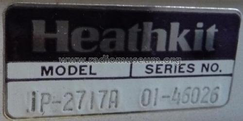
“SP” is not a typo, and it does not need “correcting” to “IP-.” The manual cover, the panel, and the part number all print SP-2717A. Heath printed it that way in 1982, in Benton Harbor, Michigan, under the Heath-Zenith ownership that followed Zenith’s 1979 acquisition of the Heath Company — a fact worth keeping straight, because it places this exact instrument at the tail end of the Heath kit-electronics era rather than in its 1960s–70s prime. By the time the SP-2717A left the factory, “Heathkit” as a customer-assembled-electronics brand was on its way out; this specific instrument is a late, factory-built artifact of that winding-down, not a kit-built survivor from the company’s peak years. Vol 1 §2 and Vol 6 carry the fuller lineage story; this volume’s job was just to establish what sits on the bench in front of you, part by part.
3.9 Quick bench-ID checklist — telling this generation apart by eye
If you’re staring into an open chassis and want to know, without a manual in hand, whether you’re looking at an SP-2717A/IP-2717A or an older family member like the IP-32, these are the hardware tells, in order of how visible they are with the case open:
Table 11 — of how visible they are with the case open
| Look for | SP-2717A / IP-2717A (this unit) | IP-32 (older sibling) |
|---|---|---|
| Gas-filled VR tubes near the reference circuitry | None — a stack of small zener diodes on the PCB instead | 2× 0A2 glass VR tubes, visibly glowing when powered |
| Selenium rectifier stacks (stacked-plate, often greenish/gray) | None — all rectification is silicon diodes | 2× selenium rectifiers present |
| Bias rectifier tube | None — silicon diodes (D7–D9) | 1× 6X4 tube |
| Control-amplifier tube type | 6AU6 | 6BH6 |
| Pass-tube suffix | 6L6GC ×2 | 6L6 ×2 (paralleled, no GC suffix) |
| Rear-panel AC output posts | Both 6.3 VAC and 12.6 VAC posts present | 6.3 VAC only |
| Solid-state board | Green PCB with a visible zener-diode row | No equivalent board — VR tubes handle reference duty in free air |
The single fastest tell, if you can only check one thing: look for the 0A2 VR tubes. Their absence, replaced by a row of small diodes on a circuit board, is diagnostic of the SP-2717A/IP-2717A generation on its own — everything else in the table above is corroborating detail. Vol 6 has the full generational comparison table including outputs, ratings, and the shared 4×27 kΩ bleeder that does not change across generations (so don’t use bleeder-resistor values as a differentiator — they’re identical family-wide).
3.10 Cross-reference — where each part shows up elsewhere in this dive
Table 12 — Cross-reference — where each part shows up elsewhere in this dive
| Part / subsystem | Defined here (Vol 3) | Circuit theory | Failure modes / refurb | Operating use |
|---|---|---|---|---|
| V1 (6AU6), V2/V3 (6L6GC) | §2 | Vol 2 (feedback loop) | Vol 5 (shorted 6AU6, tube wear) | Vol 4 (warm-up, STANDBY use) |
| ZD1–ZD10 zener stack | §2 | Vol 2 (reference) | Vol 5 (shorted zeners, cooling fix) | — |
| D1–D9 rectifiers | §2 | Vol 2 (doubler, screen, negative supplies) | Vol 5 (open/shorted diode checks) | — |
| R15–R18 bleeder | §2 | Vol 2 (minimum-load function) | — | Vol 4 §10 (not a safety discharge) |
| T1, T2 transformers | §3 | — | — | Vol 4 (STANDBY behavior) |
| B+, C–, filament outputs | §4 | Vol 2 (regulation) | Vol 5 (recap voltage ratings) | Vol 4 (hookup, floating) |
| M1, M2, S3 | §5 | — | Vol 5 (mechanical zero, recal) | Vol 4 (reading procedure) |
| S1, S2, R12, R19 | §6 | — | — | Vol 4 (operating sequence) |
| Fuse, mains input | §7 | — | Vol 5 (fuse replacement) | Vol 4 (power-up checklist) |
| R10, R14 cal pots | §6 | Vol 2 (setpoint theory) | Vol 5 (full recalibration procedure) | — |
| SP vs IP-2717 identity | §8 | — | — | Vol 1 §2, Vol 6 (full lineage) |
3.11 Full spec / device-complement reference table
Table 13 — Full spec / device-complement reference table
| Category | Item | Value |
|---|---|---|
| Identity | Model | SP-2717A |
| Manual | 595-2705-02, © 1982, Heath Company, Benton Harbor, MI | |
| Era | Heath-Zenith, 1982 | |
| Build type | Factory-assembled (likely); no kit assembly section in manual | |
| Electrically identical to | IP-2717A (radiomuseum catalog name) | |
| B+ output | Voltage | 0–400 V DC, regulated |
| Current | 0–100 mA cont., 125 mA intermittent | |
| Load reg. | < 1%, no-load to full-load | |
| Line reg. | < ±1% for ±10% AC line change | |
| Ripple/noise | < 10 mV RMS | |
| Output impedance | < 10 Ω, DC–1 MHz | |
| Active current limit | None — fuse + tube dissipation only | |
| C– (bias) output | Voltage | 0 to –100 V DC |
| Current | 0–1 mA | |
| Control | R19, 50 kΩ, special taper | |
| Protection | R20, 22 kΩ, current-limiting | |
| Filament/AC output | Option A | 6.3 V AC @ 4 A |
| Option B | 12.6 V AC @ 2 A | |
| Combined limit | ≤ 25 VA total | |
| Metering | M1 | 0–400/0–150 V DC, ±3% FS, part 407-123 |
| M2 | 0–150 mA, ±2% FS, part 407-124, in B+ cathode return | |
| S3 | VOLTMETER switch, routes M1 to B+ or C–, drives red/amber lamps | |
| Controls | S1 | AC POWER toggle, part 60-24 |
| S2 | DC ON–STANDBY toggle, part 61-9 | |
| R12 | B+ VOLTS pot, 500 kΩ | |
| R19 | C– VOLTS pot, 50 kΩ, special taper | |
| R10 | ZERO VOLTAGE ADJUST (internal cal), 500 kΩ | |
| R14 | 400 VOLT ADJUST (internal cal), 200 kΩ | |
| Devices | V1 | 6AU6, control amplifier |
| V2, V3 | 6L6GC ×2, series-pass (pentode) | |
| D1–D9 | 1N2071 silicon diode ×9 | |
| ZD1–ZD10 | Zener diode ×10, reference stack | |
| Transformers | T1 | Power (HV + screen), part 54-185 |
| T2 | Filament (6.3/12.6 V + AC out + lamp ref), part 54-184 | |
| Mains | Input | 110–130 V or 220–260 V, 50/60 Hz |
| Max draw | 150 W | |
| Fuse (120 V) | 1.5 A slow-blow, part 421-25 | |
| Fuse (240 V) | 1.0 A recommended | |
| Bleeder | R15–R18 | 4× 27 kΩ / 2 W, series, B+ bus to –300 V rail (see Vol 2) |
3.12 Where to find the schematic
This volume deliberately stays at the hardware/parts-inventory level rather than reproducing the full schematic — Vol 2 owns circuit theory. For anyone who wants the fold-out schematic and circuit-board X-ray view directly from the source, the manual itself carries both (the schematic fold-out and a circuit-board component-placement view), and independent scanned copies of the same schematic circulate under the electrically-identical IP-2717A designation at Nostalgic Kits Central and Elektrotanya — both listed below. Cross-check any third-party schematic scan against the device complement in this volume’s §2 table before trusting designator numbers pulled from a lower-resolution copy.
Sources
- Heath Company, “Model SP-2717A Regulated High Voltage Power Supply,” operation/service manual 595-2705-02, © 1982, Benton Harbor, Michigan — Specifications, Tube And Diode Complement, Circuit Description, and Parts List sections. Full manual: https://archive.org/details/Heathkit_SP-2717A_Regulated_HV_Power_Supply
- Bob Eckweiler (AF6C), “Heathkit of the Month #67 — IP-32 Bench HV Power Supply,” Orange County Amateur Radio Club, © 2015 — family lineage table (PS-1 through SP-2717A) and IP-32 circuit/device detail for cross-generation comparison. https://www.w6ze.org/Heathkit/Heathkit_067_IP32.pdf
- Radiomuseum, “Heath (Heathkit brand) IP-2717A”: https://www.radiomuseum.org/r/heath_regulated_hv_power_supply_ip_2717a.html
- “Heathkit Zenith SP-2717A Power Supply Restore,” Lazy Electrons, 2018-06-02 — restorer corroboration on the shorted-6AU6 and shorted-zener failure modes and the R19 pot-loading warning: https://lazyelectrons.wordpress.com/2018/06/02/heathkit-zenith-sp-2717a-power-supply-restore/
- Nostalgic Kits Central, IP-2717A schematic (scanned): https://www.nostalgickitscentral.com/heath/schematics/heathkit_schema_ip2717a.pdf
- Elektrotanya, “HEATHKIT SP2717A 0..400V,0.1A,0..-150V VALVE STABILISED POWER SUPPLY 1982” service manual scan: https://elektrotanya.com/heathkit_sp2717a_0..400v,0.1a,0..-150v_valve_stabilised_power_supply_1982_sm.pdf/download.html