uTracer NXT · Volume 2
uTracer NXT — Vol 2: Hardware Architecture
The NXT’s design blocks and what physically changed versus the uTracer3+/6
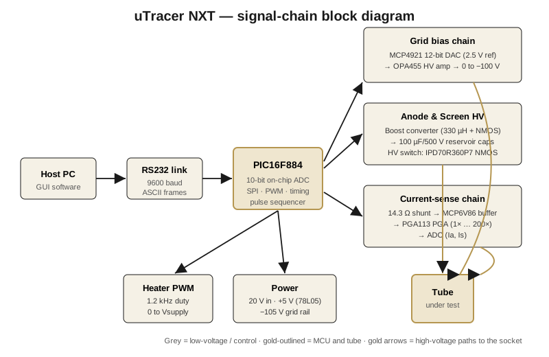
2.1 The shape of the instrument
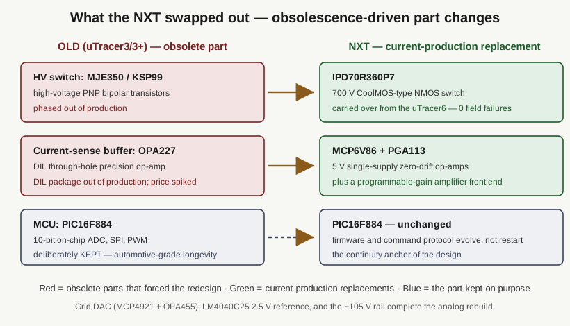
Read the block diagram left to right. A host PC running the uTracer-NXT-Gui talks over a serial link to a PIC microcontroller, and the PIC is the sequencer for everything else. On command it charges the high-voltage boost converters, sets the grid bias through a DAC-and-HV-amplifier chain, fires the high-voltage switch that connects the charged reservoir capacitors to the tube for a measurement pulse, and reads back the anode and screen currents through a shunt / programmable-gain / ADC chain. A separate heater channel runs a PWM duty cycle. That skeleton is the same in spirit as the uTracer3+ and the uTracer6 — the pulsed-capacitor idea is untouched. What changed in the NXT is the parts inside each block, and the reason they changed is component obsolescence: the OPA227 op-amp and the MJE350/KSP99 high-voltage PNP transistors that the earlier design leaned on went out of production, so Dekker took a critical look at the whole circuit and rebuilt it around current parts, folding in proven sub-blocks from the uTracer6 while he was in there. This volume walks the blocks and records what physically moved.
One framing point to keep straight throughout: the NXT is the replacement for the uTracer3+ and the current mainstream model. It deliberately targets the 3+’s voltage class — 450 V default, 500 V as an option, 350 mA default — and specifically not the uTracer6’s 1000 V territory. Every part choice below follows from living in that few-hundred-volt, few-hundred-milliamp envelope. The head-to-head generation table lives in Vol 5.
2.2 Microcontroller, sequencing, and the host link
2.2.1 The PIC16F884 — kept on purpose
The NXT keeps the PIC16F884 at its core. This is a deliberate choice, not inertia: Dekker picked it partly for longevity — the part is still listed as “recommended for automotive,” which means it will be manufactured and available for years yet. In a design whose whole motivation was escaping obsolete parts, the MCU is the one block you least want to churn, because it carries the firmware, the pulse timing, and the command protocol. Keeping it means all three evolve across generations rather than restarting from a blank sheet.
The PIC does the real-time work: it drives the boost-converter switching, sets the grid DAC over SPI, gates the HV switch for the measurement window, runs the heater PWM, and digitizes the current signals on its 10-bit on-chip ADC. The sampling scheme — before/during/after-pulse samples to separate true tube current from reservoir-cap discharge, with selectable 1× to 32× averaging — is measurement theory and belongs to Vol 3; here the point is simply that the converter is inside the same PIC that sequences everything, so there is no separate ADC chip to place or synchronize.
2.2.2 The serial link
Connectivity is a plain RS232-style serial link at 9600 baud, 8-N-1, exchanging fixed-format ASCII command/response strings (28 characters out, 38 characters back). It is not a “connected” instrument in the modern sense — there is no native USB, Bluetooth, or Wi-Fi on the board. In practice you reach it from a current PC through an FTDI USB-to-serial cable, exactly as with the earlier uTracers. The framing and command set are the province of Vol 4; the hardware fact for this volume is that the physical interface is a UART, unchanged in character from the rest of the family.
2.3 High-voltage generation and the HV switch
2.3.1 Boost converters and reservoir capacitors
Anode and screen voltages are each produced by a boost (step-up) converter: the PIC pulses an NMOS switch to pump a boost inductor and charge a reservoir capacitor up to the target plate voltage over a few seconds while the tube is held cut off. There are two 100 µF reservoir capacitors, 450 V-rated in the default build — one for the anode channel, one for the screen. Reaching the optional 500 V ceiling is conditional on fitting higher-voltage-rated reservoir caps; the rest of the circuit already has the headroom, so the 500 V option is a capacitor swap rather than a redesign.
Worth separating out here, because it is a classic point of confusion: the boost-converter switching pulse is a microsecond-scale event, and it was widened from 24 µs on the uTracer3 to 29 µs on the NXT to move the extra charge needed for the higher voltages. That microsecond figure belongs only to the DC-DC converter switching. It is not how long high voltage is applied to the tube — the tube sees the standard uTracer ~1 ms measurement pulse, which has been the family’s measurement window since the original uTracer. Do not conflate the two; Vol 3 develops the pulse theory in full.
2.3.2 The NMOS high-voltage switch — a reliability transplant
The single most consequential hardware change is which device connects the charged reservoir to the tube. The uTracer3/3+ used high-voltage PNP bipolar transistors — the MJE350 and KSP99 — for that job. Those parts have since been phased out, and they were also the weaker point of the earlier design under fault conditions. The uTracer6 had already solved this by moving to a robust NMOS high-voltage switch, and that switch earned its stripes in the field: across roughly 450 uTracer6 units deployed, the NMOS HV switch logged no reported failures.
The NXT adopts that same NMOS switch topology — the reliability advance moves down from the kilovolt model into the mainstream instrument. Because the NXT lives in a ~450–500 V envelope rather than the 6’s kilovolt one, the specific device is a 700 V-rated CoolMOS-type NMOS, the Infineon IPD70R360P7. The switch is rated to carry up to 1 A, comfortably above the NXT’s 350 mA default current ceiling, so the current headroom is not the limit — the current limit is set elsewhere, at the sense resistor. This carry-over is the clearest single example of the NXT’s stated design strategy: don’t swap obsolete parts one for one, fold in a proven block from the newer model.
2.4 The analog front end — the OPA227 problem, solved with a PGA
This is the block the whole redesign was arguably built around, because it is where the obsolescence bit hardest. The earlier uTracers conditioned the current signal with an OPA227 precision op-amp in a DIL through-hole package, and that package went out of production; availability had been a headache since COVID and the price had spiked. Rather than chase a shrinking supply of an old part, the front end was rebuilt around parts that are current and expected to stay so.
2.4.1 Sensing current across the 14.3 Ω shunt
Anode and screen currents are sensed as small voltage drops across a 14.3 Ω shunt resistor. That value is not arbitrary — it is what sets the 350 mA default current ceiling: at full-scale current the drop across 14.3 Ω is what the front end and ADC are scaled to read. Re-ranging the current envelope on the NXT is therefore a matter of changing that shunt, which is one of the jumper/resistor options the board leaves open to the builder.
2.4.2 The PGA113 programmable-gain stage
The signal off the shunt first meets a PGA113 programmable-gain amplifier, which conditions the current signal. Instead of a bank of fixed-gain channels or hand-switched ranges, the software selects a gain step to fit the signal, so the same chain resolves both small leakage/low-current readings and full plate currents against the 10-bit ADC. This is what buys the NXT usable resolution across its whole current span from a single, modest converter: the PGA does the ranging, the ADC does the counting.
2.4.3 The MCP6V86 output stage and true-ground referencing
The PGA113 feeds the MCP6V86, a single-supply, 5 V rail-to-rail zero-drift op-amp that replaces the OPA227 — a current-production part in a package the design can rely on. Because it runs from a single 5 V rail, getting it to read signals that sit at true circuit ground takes a trick: a pull-down to the −105 V rail shifts the reference so the front end measures against real ground rather than against the positive rail. That −105 V rail (below) does double duty for exactly this reason — it references the analog front end as well as biasing the grid. Between the shunt, the PGA113, and the MCP6V86, the front end is now entirely current-production silicon — the OPA227 dependency is gone.
2.5 The grid-bias chain
Control-grid bias is generated by a DAC feeding a high-voltage amplifier. In the NXT that is a 12-bit MCP4921 SPI DAC spanning 0–5 V, referenced to an LM4040C25 2.5 V precision shunt reference, feeding an OPA455 high-voltage op-amp wired as a −20× inverting stage. Twenty times the DAC’s 5 V swing, inverted, gives the 0 to −100 V grid range in the default design; later development pushed the extended range to roughly −140 V with additional circuit tweaks beyond the default. The grid amplifier runs against the −105 V negative rail, which is why that rail exists.
The NXT provides negative grid bias only in its documented design (0 to −100 V, extended to ~−140 V in later development), and that is a deliberate scope decision that follows straight from the target market. It is aimed at ordinary receiving and audio tubes, which are characterized in the negative-grid region, so its grid chain spans only the negative range.
2.6 Power architecture
The NXT derives its low-voltage rails on-board:
- an on-board +5 V logic rail, feeding the PIC, the DAC, the reference, and the low-voltage analog parts; and
- a −105 V negative rail, boost-generated on-board, used both to bias the grid amplifier and to reference the current-sense front end to true ground.
The high plate voltages themselves are not “rails” in the supply sense — they are the transient charge on the two 100 µF reservoir capacitors, pumped up by the boost converters only when a measurement is pending and dumped into the tube during the ~1 ms pulse. That is the whole point of the pulsed architecture: there is no continuous multi-hundred-volt, high-current supply to build, heat-sink, or fear. The heater/filament channel is driven as a PWM duty cycle at 1.2 kHz, and it can supply either DC or AC (AC through a transformer, for directly-heated tubes that want it).
2.7 Physical form — the through-hole kit
Physically the NXT stays true to the family: a predominantly through-hole PCB (a few SMD parts such as the op-amps and DAC aside), meant to be assembled by hand rather than reflowed. The board is deliberately dimensioned to the uTracer3 PCB footprint, close enough that Dekker describes it as a “drop-in replacement for the uTracer3 with minimal changes” — the terminal positions and mounting line up with the earlier mechanical layout. Small build touches follow from the hand-solder intent: the inductors are mounted vertically on modified pin headers to make them easier to solder in.
Crucially for a curve tracer, the board leaves jumper and resistor options open so the builder can re-range current, voltage, and grid bias without a board respin — the 14.3 Ω sense resistor for current, the reservoir-cap rating for the 500 V option, and the grid divider for the extended bias range are all builder-selectable positions rather than fixed values. The build itself and its calibration are Vol 4.
2.8 The measurement envelope
Pulling the numbers together for the NXT itself — the side-by-side against the 3+ and the 6 is Vol 5:
Table 1 — Pulling the numbers together for the NXT itself — the side-by-side against the 3+ and the 6 is Vol 5
| Parameter | Default | Notes / extended |
|---|---|---|
| Anode / screen voltage | 450 V | 500 V option with higher-rated reservoir caps |
| Reservoir capacitors | 2 × 100 µF, 450 V | charged by the boost converters; the 500 V option raises the cap rating |
| Anode / screen current | 350 mA | set by the 14.3 Ω shunt; HV switch rated to 1 A |
| Control-grid bias | 0 to −100 V | extended to ~−140 V in later development |
| Negative supply rail | −105 V | grid bias + front-end ground referencing |
| Heater / filament | PWM at 1.2 kHz | DC, or AC via transformer for directly-heated tubes |
| Boost-converter switching pulse | 29 µs | (24 µs on the uTracer3) — a DC-DC detail, not the tube pulse |
| Measurement pulse into the tube | ~1 ms | standard across the whole uTracer family (Vol 3) |
| HV switch device | IPD70R360P7 | 700 V NMOS, carried over from the uTracer6 |
The net picture: same pulsed idea, same PIC16F884 and serial interface, same solder-it-yourself board on the uTracer3 footprint — with a modernized, parts-available analog front end (MCP6V86 + PGA113 in place of the OPA227) and the uTracer6’s NMOS high-voltage switch underneath it, all sized for the 450–500 V / 350 mA mainstream envelope the NXT was built to own.