Curve Tracers — Overview & Primer · Volume 4
Curve Tracers — Vol 4: Reading and Using the Curves
β, transconductance, the Early effect, breakdown, saturation, matching — and the traps
This is the volume the rest of the primer builds toward. Vol 1 said what a curve tracer is, Vol 2 laid out where the instruments came from, and Vol 3 walked through how the sweep, the step generator, and the X-Y display conspire to draw a family of curves. Here you learn to read that picture — to look at a fan of traces and pull real numbers, with units, off the screen, and to know when the picture is lying to you.
The organizing idea is worth stating once, plainly: a curve tracer measures a device, but it teaches you a model. A single meter reading — an hFE of 180, a gm of 5 mS — is a point. The tracer shows you the whole surface that point sits on, so you can see how the parameter moves as the device runs hotter, harder, and closer to its limits. Every skill in this volume is a way of turning a shape into a slope, a spacing, or a corner, and then attaching a number to it.
We work through the bipolar transistor’s output family first — because everything else is a variation on it — then the diode, the FET, and the vacuum tube, then the specific job of matching devices, and finally the pitfalls that produce misleading curves. Throughout, the specific instruments in this hub — the semiconductor tracers (the VBA Curve Tracer and the vintage Heathkit IT-3121) and the pulsed-HV tube tracers (the eTracer, uTracer6, and uTracer NXT) — are named where the reading skill depends on what the instrument can actually do.
4.1 Reading a BJT output family
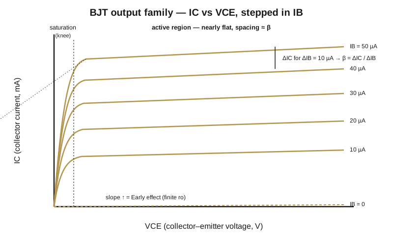
The bipolar output family plots collector current IC (vertical) against collector–emitter voltage VCE (horizontal), with one curve per base-current step. The step generator hands the base a fixed staircase of current — say 10 µA per step, five or ten steps — and for each tread it sweeps VCE from zero up to whatever ceiling the range switch allows, dragging the electron beam across the screen once per sweep. What you get is a fan. Five features live on that fan, and each one is a different measurement.
4.1.1 Cut-off and leakage — the bottom of the plot
Cut-off is the lowest trace: with IB = 0 the transistor is turned off and passes only a small leakage current, so that curve hugs the horizontal axis. It is easy to ignore, and you should not, because it is a free health check. A curve that sits noticeably above the axis at IB = 0 is telling you the device is leaky — collector-to-emitter leakage (ICEO) that a single β reading at a healthy bias point would never reveal. On a small-signal silicon part you expect that bottom trace to be visually pinned to the axis, leakage in the nanoamps to low microamps. See it lift off the axis by a division and you are looking at a part that has been cooked, contaminated, or is simply a leaky germanium device behaving as germanium does — old germanium transistors routinely show tens of microamps of ICEO at room temperature and far more when warmed by a fingertip. The tracer makes that visible instantly; watching the bottom curve climb as you warm the part with your finger is the classic germanium-leakage demonstration.
4.1.2 The saturation knee
The saturation knee is the steep, near-vertical rise at the far left, where VCE is only a few tenths of a volt. Here the collector–base junction has gone forward-biased, the transistor is fully on, and VCE physically cannot fall any further no matter how much base drive you pour in. For a small silicon device the knee sits around VCE(sat) ≈ 0.1–0.3 V; for a saturated power device it may be 0.5 V or more, and that number is not cosmetic — in a switching application VCE(sat) times the load current is the conduction loss. A device carrying 3 A with a VCE(sat) of 0.4 V is dissipating 1.2 W just being “on.”
Two things to read off the knee. First, its voltage: where does the curve leave the vertical and bend into the active plateau. Second, the slope of the rise itself, which is the collector–emitter on-resistance in saturation, RCE(sat) = ΔVCE / ΔIC down in that region — a nearly vertical knee is a low on-resistance, a lazily leaning one is a higher one. A knee that is soft and rounded where it should be crisp is a common symptom of a tired power transistor.
4.1.3 The active region and β
The active region is the broad, nearly-flat plateau where the curves run left-to-right across most of the screen. This is where the transistor works as a linear amplifier: IC is set almost entirely by IB and barely depends on VCE. The vertical spacing between adjacent curves is the current gain. Because each step is a known increment of base current, the DC current gain at any point is
β = h
FE= ΔIC/ ΔIB
Concretely: if the step generator is set to 10 µA/step and two adjacent curves are separated by 1.8 mA of collector current, then β ≈ 1.8 mA / 10 µA = 180 at that operating point. That is a large-signal, “how far apart are the curves” number — the DC β. The small-signal gain hfe (lower-case subscripts) is the spacing between two curves that are only an incremental step apart at a fixed collector current, and on a well-behaved device in the middle of its range the two numbers are close enough that people use them interchangeably; at the current extremes they part company, which is exactly what the tracer is for.
The single most useful habit here is to read the spacing in more than one place. Measure it low on the screen, at a milliamp or two, and again high on the screen near the device’s rated current. If the curves are evenly spaced top to bottom, β is constant across that range. If they bunch together at the top — spacing shrinking as IC climbs — you are watching β roll off as the device runs out of headroom, the high-current gain droop that every power transistor has and that no single hFE figure will warn you about. Read low and you might record β = 200; read high and the same part might be delivering β = 60. Both are true; the circuit sees whichever one corresponds to where it biases the device. This is the whole argument for a picture over a number, made concrete: the tracer lets you see β sag before you design around a gain the part cannot hold.
There is a small-signal cousin worth naming while we are here. The bipolar transistor also has a transconductance, gm = ΔIC / ΔVBE, which for a BJT is not something you step-and-read the way you do for a FET — it is set by physics, gm = IC / VT, where VT ≈ 26 mV at room temperature. At IC = 1 mA that is gm ≈ 38 mS, and it scales linearly with collector current. The tracer does not hand you gm off a BJT family directly, but knowing it comes straight from IC is why the collector current, not the transistor “type,” sets the gain of a bipolar stage.
4.1.4 The Early effect
The Early effect is the gentle upward slope of those “flat” active-region curves. Ideally the active curves would be perfectly horizontal — a transistor that is a perfect current source, with infinite output resistance. In reality they tilt up slightly: as VCE rises, the reverse-biased collector junction’s depletion region widens, the effective base gets thinner, and IC creeps up. Extrapolate the active curves backward to the left and they converge, more or less, on a single point on the negative-voltage axis. The magnitude of that intercept voltage is the Early voltage, VA, and it is a figure of merit: small-signal parts might show VA of 50–150 V, ideal current-source-grade parts far more.
What you actually care about at a given operating point is the output resistance that slope implies:
r
o= ΔVCE/ ΔIC(along one active curve)
and it ties to the Early voltage as ro ≈ VA / IC. Worked: a curve that climbs 0.1 mA over a 10 V span of VCE has ro = 10 V / 0.1 mA = 100 kΩ at that current. A steeper slope means a lower ro and a smaller VA — which matters enormously when the transistor is used as a current source, a cascode, or the tail of a differential pair, where the whole point is a high output impedance. A tracer shows this instantly as a fan that is not quite parallel: parallel-and-flat is a high Early voltage, a fan that visibly splays open toward the right is a low one.
4.1.5 Breakdown
Breakdown is at the far right. Push VCE high enough and the top curve suddenly hooks upward and the current runs away — that corner is BVCEO, the collector–emitter breakdown voltage with the base open. There are cousins that depend on how the base is terminated (BVCBO with the emitter open, BVCES with base shorted to emitter, generally higher than BVCEO), and a curve tracer with a base-terminal option can show you each. On the instrument you creep up on it deliberately: set the series/load resistor high so that when the device does break over, the runaway current is limited by that resistor and you read the breakdown voltage off the horizontal scale without vaporizing the junction. Start with the current-limit conservative and the voltage low, and open the voltage up only as far as you need — the load line drawn by that series resistor is your safety net. This is the one measurement where the discipline is not optional: an unlimited supply into a device in avalanche is a dead device, every time.
4.2 Reading a diode
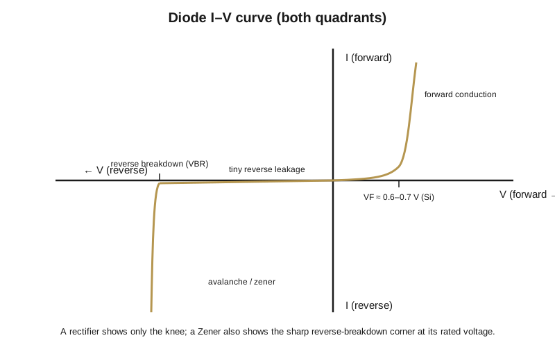
A two-terminal diode gives a single curve, no stepped family — there is no control terminal to step. That single curve still carries four numbers.
The forward knee. Forward-biased, the diode stays near zero current until it reaches its turn-on knee — about 0.6–0.7 V for a silicon junction, ~0.3 V for germanium, ~0.25 V for a Schottky, and anywhere from 1.8 V (red) to directly off the horizontal scale at whatever forward current you dial in, and the shape of the turn-on tells you more than a meter’s diode-test can: a soft, early, sloppy knee flags a leaky or degraded junction.3.4 V (blue/white) for an LED, whose knee voltage is essentially its band-gap and rises with the color. Above the knee the current climbs steeply and roughly exponentially. The tracer reads VF
Series resistance at high forward current. Follow the forward curve up past the knee and it eventually stops being a clean exponential and straightens into a line leaning to the right — that lean is the diode’s bulk series resistance RS, the ΔV/ΔI slope up in the high-current region. On a power rectifier that resistance is what turns forward current into self-heating.
Reverse leakage and breakdown. Reverse-biased, the diode passes only a tiny leakage current along the horizontal axis — nanoamps for a healthy small-signal silicon part — until, for a Zener or avalanche diode, it reaches its rated reverse breakdown and the curve drops sharply and vertically at VBR. A plain rectifier operated within its ratings shows only the forward knee; a Zener shows both corners, and the tracer reads its breakdown voltage directly off the horizontal scale — dial the reverse current to the Zener’s rated test current (say 5 mA) and read the voltage there, because the “5.1 V” on the part is specified at a current, not at zero. The sharpness of that reverse corner is itself a grade: a crisp vertical knee is a healthy Zener or avalanche part; a soft, rounded reverse bend, or leakage that is visibly above the axis before breakdown, flags a degraded device. A forward knee in the wrong place, a soft reverse corner, and lifted leakage are the three diode failure signatures, and all three are obvious on the tracer and invisible to a go/no-go tester.
One temperature note, because it shows up as drift while you watch: a forward-biased silicon junction moves about −2 mV/°C, so a diode curve that slides leftward as the part warms under sustained forward current is normal physics, not a fault. Zener knee tempco flips sign around 5–6 V (below it the coefficient is negative, above it positive), which is why the classic low-tempco references cluster near 5.6 V.
4.3 Reading a FET
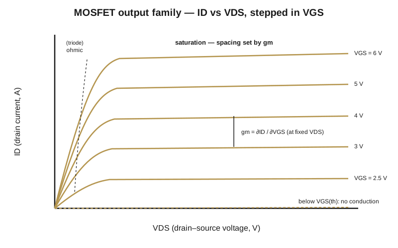
A FET’s output family plots drain current ID against drain–source voltage VDS, stepped in gate voltage VGS — not gate current, because the gate of a MOSFET or JFET draws essentially no DC current. That one change, stepping a voltage instead of a current, is the deepest difference between reading a FET and reading a BJT, and it is why the step generator’s voltage-step mode (Vol 3) exists. The shape rhymes with the BJT’s, but the vocabulary shifts.
The ohmic (triode) region. Near the origin, at low VDS, the curves rise steeply and almost linearly out of zero: here the FET behaves like a voltage-controlled resistor, and the slope of that rise is 1/RDS(on), the on-resistance that is the headline number for a switching MOSFET. Read it as RDS(on) = ΔVDS / ΔID down near the origin, at the highest gate drive — a power MOSFET fully enhanced (VGS well past threshold) might show 40 mΩ there, and that resistance times the square of the drain current is its conduction loss. Note that RDS(on) is gate-drive dependent: the ohmic slope gets steeper (lower resistance) as you step VGS higher, which is exactly why data sheets specify RDS(on) “at VGS = 10 V.”
Pinch-off and the saturation plateau. Past the pinch-off boundary the curves bend over and flatten into the saturation region used for amplification — the FET equivalent of the BJT’s active region. The curves here are flatter than a BJT’s are and, like the BJT, tilt up slightly with a finite output resistance (the FET’s analog of the Early effect, from channel-length modulation).
Transconductance. The key small-signal parameter for a FET is transconductance, gm — how much drain current you get per volt of gate drive — read from the vertical spacing between adjacent curves in the saturation region at a fixed VDS:
g
m= ΔID/ ΔVGS(at constant VDS)
Worked: if the gate steps are 0.5 V apart and two adjacent saturation curves are separated by 4 mA at your chosen VDS, then gm = 4 mA / 0.5 V = 8 mS (8 mA/V) at that operating point. Unlike a BJT’s β, which is roughly constant, a FET’s gm rises with drain current, so the curves spread apart as you go up the screen — the opposite visual of the BJT’s high-current bunching. Reading the spacing at two heights lets you see how much gain the device gains as you bias it harder.
Threshold and the transfer curve. For a JFET or depletion-mode MOSFET you can read the pinch-off / threshold voltage directly: it is the gate voltage of the curve whose drain current has just collapsed to zero. This is where the step generator’s polarity and offset controls stop being a convenience and become a hard requirement. An enhancement-mode MOSFET does not conduct at all until VGS passes a threshold that is often several volts positive (an n-channel logic-level part around +1 to +2 V, a standard part +3 to +4 V), so the instrument must be able to offset the gate staircase positive or it will show you a dead, non-conducting part that is in fact perfectly good. This is a concrete instrument limitation to know before you trust a “bad FET” verdict: the vintage Heathkit IT-3121 could not offset its gate steps positive without the well-known modification, whereas the fully-analog VBA Curve Tracer, designed in the modern era with enhancement MOSFETs squarely in scope, handles positive gate offset by design. Reach for the right instrument, or add the offset, before you condemn the device.
4.4 Reading a vacuum tube plate family
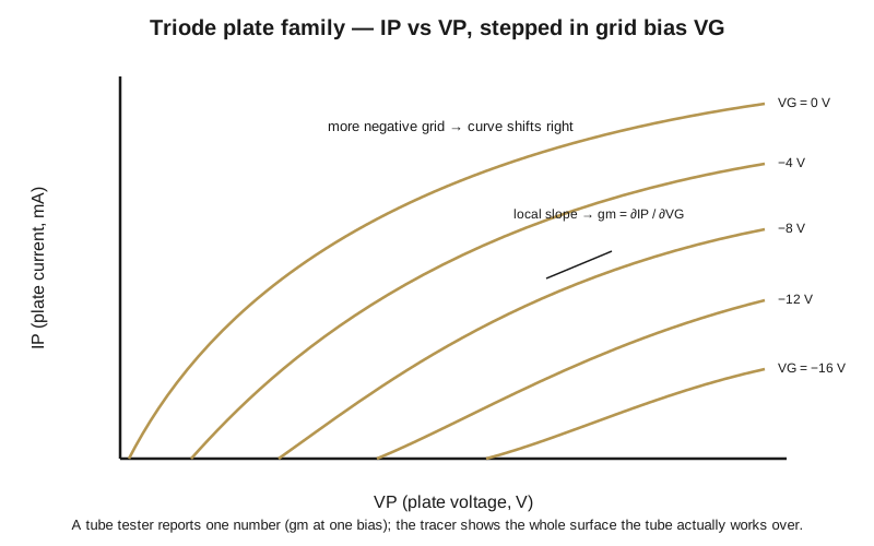
The pulsed-HV tube tracers in this hub — the eTracer (Essues, Taiwan; anode to 750 V), the kilovolt uTracer6 (Dekker, to 1000 V), and the current-mainstream uTracer NXT (Dekker) — draw the same kind of picture for a vacuum tube, and the reading skill transfers with a change of names. A triode plate family plots plate current IP (vertical) against plate voltage VP (horizontal), one curve per step of grid bias VG. Because the grid is driven negative and draws no current, the family is stepped in grid voltage, exactly like a FET — the vacuum triode is the FET’s spiritual ancestor.
Three numbers come off a tube family, and the tube world names them differently but they are the same slopes you already know:
- Transconductance / mutual conductance, g
m= ΔIP/ ΔVGat fixed VP— the vertical spacing between grid-step curves, exactly the FET’s gm. Tube data sheets quote it in µmhos (micromhos) or millisiemens; a small-signal triode like a 12AX7 runs about 1,600 µmho (1.6 mS), a 6L6 output pentode roughly 6,000 µmho. This is the number a mutual-conductance tube tester like Jeff’s Heathkit TT-1 reports as a single figure at one bias point — the tracer shows the whole surface that figure was plucked from. - Plate resistance, r
p= ΔVP/ ΔIPalong one curve — the slope of a single trace, the tube’s output resistance, the analog of the BJT’s ro. A 12AX7 sits near 62.5 kΩ. - Amplification factor, µ = ΔV
P/ ΔVGat fixed IP— the horizontal spacing between curves at a constant current, and the three tie together as µ = gm× rp(the tube’s own version of the same relationship). A 12AX7’s µ ≈ 100 falls right out of 1,600 µmho × 62.5 kΩ.
Matching a push-pull output pair, spotting a gassy or low-emission tube (its whole family sits low and the curves crowd together), and finding a tube whose gm has faded are all the same overlay-and-compare skill you use on transistors, just at a few hundred volts of pulsed plate sweep instead of tens of volts of DC collector sweep.
4.5 Matching devices — the job the tracer is uniquely good at
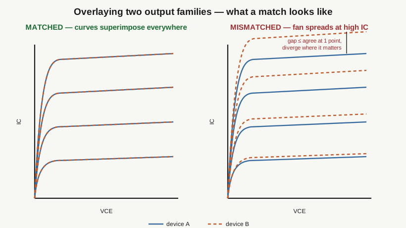
Why match? Differential pairs, push-pull output stages, current mirrors, and banks of paralleled power devices all depend on two — or four, or eight — devices behaving identically. A current mirror copies a current only as well as its two transistors match; a differential pair’s input offset voltage is set by how closely its pair tracks; paralleled power transistors share current only if their VBE and gain match, or one hogs the load and cooks. And a single β or gm reading that agrees at one bias point does not make two parts a match — the caution Vol 2 raised about tube testers applies just as forcefully to semiconductors. Two transistors can share the same nominal gain at 1 mA and diverge badly at the 500 mA where your output stage actually runs them.
How the tracer does it. Overlay one device’s family on the other’s — either by displaying both on the same screen (a dual-station tracer, or one part then the other with the display in a persistence/storage mode) or by capturing each and comparing the traces. Matched devices produce superimposable families: the curves land on top of each other across the whole range, not just at one point. That is the discipline the figure above is trying to burn in — the mismatched pair on the right agrees perfectly at the bottom of the screen and splays wide open at the top, which is precisely the failure a one-point tester passes and a designer curses later. On the digitizing tracers here you overlay the captured data directly: the VBA Curve Tracer puts both families on the host display, and the tube tracers — eTracer, uTracer6, uTracer NXT — capture each tube’s curves to the PC so a matched quad can be compared trace-for-trace and even exported. This is the standard way to select complementary NPN/PNP pairs, matched quads for an audio output stage, and matched tubes for a push-pull amplifier — and it is something no single-number tester can do honestly, because “same number at one point” and “same curve everywhere” are different claims.
4.6 Common measurements, at a glance
The parameters you pull straight off the screen:
Table 1 — The parameters you pull straight off the screen:
| Parameter | Device | Where you read it |
|---|---|---|
| β / h | BJT | Vertical spacing of active-region curves ÷ step size |
| V | BJT | Voltage at the saturation knee (~0.1–0.3 V, small Si) |
| R | BJT | Slope of the near-vertical saturation knee |
| BV | BJT | V |
| Early voltage V | BJT | Slope of the active curves (back-extrapolation) |
| Leakage (I | BJT / diode | Current above the axis at zero drive / reverse bias |
| g | BJT | Set by I |
| V | Diode | Voltage at the forward knee, at a stated current |
| R | Diode | Slope of the forward curve well above the knee |
| V | Diode | Reverse-breakdown corner, at rated test current |
| g | FET | Vertical spacing of saturation curves ÷ V |
| R | MOSFET | Slope in the ohmic region near the origin, at high V |
| V | FET | V |
| g | Tube | Vertical spacing / single-curve slope / horizontal spacing |
4.7 Pitfalls — how a tracer lies to you
The instrument is honest about what it measures; it is up to you not to measure the wrong thing. These are the traps that turn a good tracer into a source of confident wrong numbers.
- Thermal droop and runaway. Leave a power device dwelling at high dissipation and it heats during the sweep, and the curves drift — a silicon BJT’s β climbs with temperature so the fan opens up as it warms, and a hot device left dwelling can slide into thermal runaway and destroy itself on the bench. This is why nearly every tracer sweeps from a rectified line or pulses rather than holding DC: the device is only at full power for part of each cycle. Keep the peak-power / series-resistor control conservative, read quickly, and do not sit on a hot part. The drift is real physics, not an instrument fault — but a β you read off a curve that is still climbing is a β at an unknown temperature.
- Reading a parameter off the wrong region. β read down in the saturation knee, or up in the last division before breakdown, is not the β your circuit sees. Read it in the flat active region, at a collector current and voltage representative of the actual operating point. The same goes for g
m(read it in saturation, not the ohmic region) and ro(read it where the curve is genuinely flat). - Parallax and coarse graticule reading. On a CRT tracer the trace floats a few millimeters in front of the graticule, so reading spacing from an angle costs you accuracy — a couple of tenths of a division of parallax is a 10–20 % error in a β pulled from two closely-spaced curves. Line your eye up square to the screen, and prefer reading a large spacing (several divisions) over a small one. On the digitizing tracers this trap disappears — the host reads the numbers off the captured data — which is a quiet but real argument for them.
- Forgetting the scale factors. A curve is meaningless without the current-per-division and volts-per-division that go with it. On a scope-driven rig — the Heathkit IT-3121 or the VBA Curve Tracer feeding an external X-Y scope, or any octopus-plus-scope setup — you set those scale factors on the scope yourself, and a wrong V/div or A/div makes every number wrong by exactly that factor. Write the settings down with the curve.
- Under-driving a MOSFET (or a tube). Trying to trace an enhancement MOSFET without a positive gate offset shows a dead, non-conducting device — an instrument limitation, not a bad part (the reason for the Heathkit IT-3121 offset modification, and why the VBA Curve Tracer handles positive offset natively). The tube equivalent: fail to supply the right grid-bias range and a good tube looks cut-off or wide-open.
- In-circuit surprises on an octopus. When you use the signature-tester / octopus form of the tracer (Vol 1) on a component still soldered to a board, a signature that looks “wrong” may just be other parts on the same node loading the reading. The octopus’s strength is comparison to a known-good board, node by node — not absolute reading of an in-circuit part.
- Exceeding the safe operating area. The tracer will happily drive a device past its safe operating area — the combined voltage-and-current limit the part can survive — if you let it. Start high-resistance and low-voltage, watch the load line the series resistor draws, and open up only as far as the measurement needs. The discipline is identical whether you are on ±200 V / 1 A of the IT-3121’s semiconductor sweep, the VBA’s analog sweep, or several hundred volts of pulsed plate voltage on a tube tracer — and it is the same discipline that lets you read BV
CEOor a Zener knee without a puff of smoke.
A closing calibration on the numbers in this volume: they are illustrative, chosen to make the arithmetic land — a real 2N3904 or IRFZ44 or 12AX7 will read what it reads, and the point of the instrument is that you no longer have to trust the round number on the data sheet. You can put the part on the tracer and see the surface it actually lives on. With that reading skill in hand, Vol 5 turns practical: which real instrument to reach for, and when to buy vintage Tektronix iron versus build a modern DIY tracer.